

1. Introduction
Many microelectronic devices are stretching their limits towards miniaturization the capacitance density and the size of the capacitor. Tantalum capacitor, made from tantalum powder (in the form of compacted anode), has been a major contribution to the miniaturization of electronic circuits1) because the higher capacitance per gram of tantalum powder, the smaller tantalum chip. Along with this miniaturization of electronic circuits, tantalum (Ta) capacitors have been on the market for more than half a century and they still continue to grow due to its large demands worldwide and advantages such as high volumetric efficiency, low temperature coefficient of capacitance, high stability and reliability2,3). Thus, the Ta capacitors have been used in the special applications such as military, aerospace, and medical4).
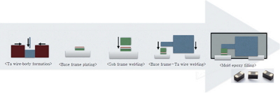
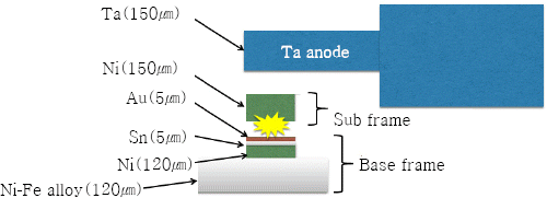
A tantalum capacitor manufacturing process is depicted in Fig. 1. First, Ta wire is embedded into the Ta powder and Ta body is formed by a frame. Second, a base frame is formed by coating several layers. Third, a sub frame is welded on the base frame. Nickel is used as the sub frame to provide excellent weldability and electrical connectivity between a base frame and Ta wire. In addition, Au-Sn-Ni alloy is used as the base frame to provide corrosion resistance. Fourth, the joined body of sub and base frame is welded with Ta wire. Finally, mold epoxy is filled in a Ta outer frame. During the Ta manufacturing process, the sub frame needs to be welded with base frame In addition to the sub frame welding, tantalum anode needs to be welded with sub frame.
Currently, arc welding has been used to weld base frame and sub frame. For arc welding, a welding electrode is a crucial component5,6).
As the tantalum capacitor is miniaturized, a weld size is diminishing for the base and sub frame welding. Thus, the size of welding electrode also needs to be diminished to generate a small weld size. Since there is a size limit to manufacture the welding electrode, arc welding may be difficult to apply the base and sub frames welding as long as the miniaturization trend exists. In addition, many manufacturers want to improve manufacturing productivity. The manufacturing productivity is closely related with processing time. Arc welding must require a contact between the welding electrode and materials. The contact time is burden to decrease processing time, therefore, and the productivity.
Laser welding may solve these problems since it requires no contact7-12). In addition, since laser spot size can be minimized in the order of 1 ╬╝m as modifying optical design, laser welding can be beneficially used for high-precision micro welding. Furthermore, high speed scanning system may help to improve the processing time. Therefore, in this study, laser spot welding is applied to weld the base and sub frame of Ta capacitor.
Many researches are focus on improvement of material properties and the capacitors performances. However, despite the importance of the manufacturing technology, few researchers paid attention to Ta capacitor manufacturing technology. Villarreal et. al.3) investigated a method for cleaning tantalum capacitors terminals, using the technique of selective ablation by pulsed laser with the aid of LIBS technique. From this study they characterize capacitors and determine the resin composition and possible contaminants adhered. More fundamental manufacturing research has been done by Patwa et. al.13). Laser percussion drilling was performed using an IR pulsed disk laser in a 1 and 2mm thick Ta plate to create an array of high aspect ratio holes of 60:1 In this study, the process parameters were optimized and a hybrid nozzle, with both horizontal and vertical gas flow, was developed and implemented.
In this paper, first experimental set-up and material used are mentioned. Second, experimental results and discussion are followed. Finally, conclusion will be presented.
2. Experiments
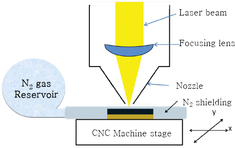
Experimental set-up is shown in Fig. 3. Laser welding head is used. N2 gas is used to prevent oxidation. N2 gas is flowing with certain speed from a gas reservoir to the interaction region. This system is designed with a single mode CW fiber laser with the wavelength of 1.070 nm. Its maximum laser power is 500 W. The laser beam is fiber delivered and the core-fiber diameter is 10 ╬╝m. The measured spot size at the focus position is 22 ╬╝m and Gaussian beam shape is used. Spot welding is performed with suitable fume exhaust systems in a clean and dust free environment. In this study, laser power is fixed as 200 W.
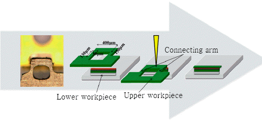
Welding geometry is shown in Fig. 4 and lap joint is used. Upper workpiece is attached to a main body by a connecting arm. The size of the upper workpiece to be welded is 400 ╬╝m (L) ├Ś 150 ╬╝m (W) ├Ś 150 ╬╝m (H). The size of the connecting arm in the upper workpiece is 130 ╬╝m (L) ├Ś 50 ╬╝m (W) ├Ś 150 ╬╝m (H). The proposed welding geometry makes the upper workpiece unmovable during the welding process. When laser energy is applied onto the upper workpiece, the connecting arm will be detached from the main body due to the evaporation.
Fixed laser parameters for experiments are tabulated in Table 1. Laser irradiance time and energy are shown in Table 2. In these experiments, laser irradiance time is the only control variable. The concept of laser irradiance time is shown in Fig. 5. Since the continuous laser is used, laser power is fixed as 200 W. Laser energy irradiated for each experiment is varied based on the laser irradiance time and can be expressed as follows
Table┬Ā1
Fixed laser parameters for experiments
| Power [W] | Intensity [W/cm2] | N2 [l/min] | Shot number | Focal position [mm] |
|---|---|---|---|---|
| 200 | 52613204.33 | 20 | 1 | 0 |
Table┬Ā2
Laser irradiance time and energy for experiments
| Time [ms] | Energy [mJ] |
|---|---|
| 5 | 1000 |
| 10 | 2000 |
| 11 | 2200 |
| 12 | 2400 |
| 13 | 2600 |
| 14 | 2800 |
| 15 | 3000 |
| 16 | 3200 |
| 17 | 3400 |
| 18 | 3600 |
| 19 | 3800 |
| 20 | 4000 |
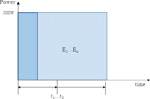
where Eirradiance is irradiated laser energy, P is laser power, and tirradiance is laser irradiance time.
3. Results And discussion
Results of spot welding are shown in Fig. 6. Due to the particular welding geometry design, interesting shapes of resulting weldments can be observable. Four different shapes are presented : 1) no melting upper workpiece, 2) asymmetric spherical-shaped weldment, 3) symmetric weldment, 4), excessive weldment.
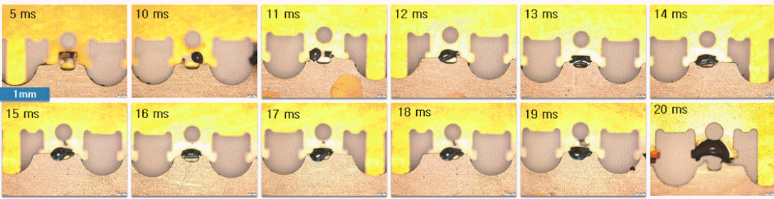
When the irradiance time is 5 ms, no phase change is observed. Only blacken surface can be observed on the upper workpiece. From this result, there is not enough energy to melt the upper workpiece.
When the irradiance time is 10 ms and 11 ms, the upper workpiece is melted and resolidified as a spherical-shaped weldment. Furthermore, the spherical-shaped weldment is attached only on the right-hand side for the irradiance time of 10 ms. For the irradiance time of 11 ms, the spherical-shaped weldment is attached only on the left-hand side. Unequal surface tension applied both on the right and left connecting arms may result in this phenomenon. Based on this observation, temperature in the molten material on the upper workpiece may be not distributed symmetrically. Asymmetric temperature distribution may lead to asymmetric surface tension distribution so that the spherical-shaped weldment can be form either on the right or left connecting arm. This asymmetric temperature distribution may be due to the development of melt pool since unstable melt pool flow can be observed while developing the melt pool. This unstable and developing melt pool can be observed during a transition from the initial stage to the final stage of melt pool development8).
The author suspect the irradiance time between 10 ms and 11 ms, where asymmetric spherical-shaped weldment observed, is the transition stage since this regime is placed between the irradiance time leading to no melting upper workpiece and the irradiance time leading to symmetric weldment. Furthermore, optical alignment can affect the formation of asymmetric spherical-shaped weldment, since optical misalignment of laser beam could create asymmetric temperature distribution. Therefore, the given irradiance time is not enough to create symmetric temperature distribution in the molten material on the upper workpiece.
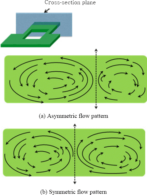
When the laser irradiance time is applied more than 11 ms and less than 20 ms, the weldment is attached on both side of the connecting arm. This symmetric weldment seems more stable than the asymmetric spherical-shaped weldment. From this result, we can guess that there is symmetric temperature distribution in the molten material during the laser spot welding process. Thus, when the laser irradiance time is more than 11 ms, symmetric temperature distribution may be formed in the molten material. Moreover, due to the symmetric temperature distribution, a flow pattern in the molten material may also be symmetric. The flow pattern the author may think of is shown in Fig. 7. This symmetric temperature distribution may be achieved since a laser-material interaction zone reaches its thermal equilibrium between the heat input from the laser source and energy loss by heat transfer and phase change.
The laser irradiance time of 20 ms shows excessive weldment. More weldment can be created than the asymmetric spherical-shaped weldment and symmetric weldment. This may due to excessive heat is applied so that more material on the upper workpiece is melted.
4. Conclusions
Tantalum capacitor has been a major contribution to the miniaturization of electronic circuit. Despite the importance of the manufacturing technology, few researchers paid attention to Ta capacitor manufacturing technology. Arc welding has been used to weld base frame and sub frame. However, there exists a limit to use the arc welding since the downsizing of the weldment depends on the size of welding electrode and the contact time may prevent from improving processing time so that productivity. Hence, this study proposes laser spot welding to solve these problems. Using CW IR fiber laser, laser spot welding is applied on the lap joint geometry with the variation of laser irradiance time. Four different shapes, such as 1) no melting upper workpiece, 2) asymmetric spherical-shaped weldment, 3) symmetric weldment, and 4), excessive weldment, are presented. These different shapes may be due to the different temperature distribution and the flow pattern in the molten material on the upper workpiece depending on the laser irradiance time.
 PDF Links
 PubReader
 ePub Link
 Full text via DOI
 Download Citation
 Print
Print