


1. Introduction
2. Experimental method
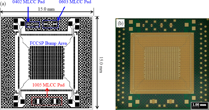
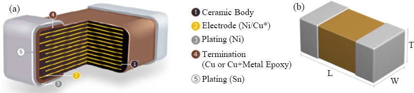
2.1 Substrates and MLCC components for semi- conductor packaging
Fig.┬Ā1
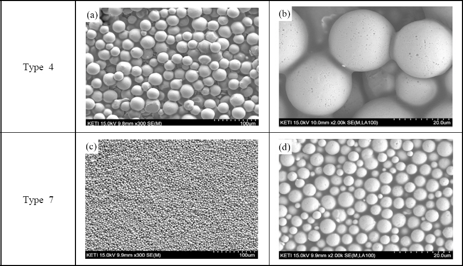
2.2 Pb-free solder paste and printing process
Table┬Ā1
Fig.┬Ā3
2.3 Hot air reflow soldering and vacuum soldering
2.4 Measurement of void content at solder joints and shear strength test
3. Experimental Results
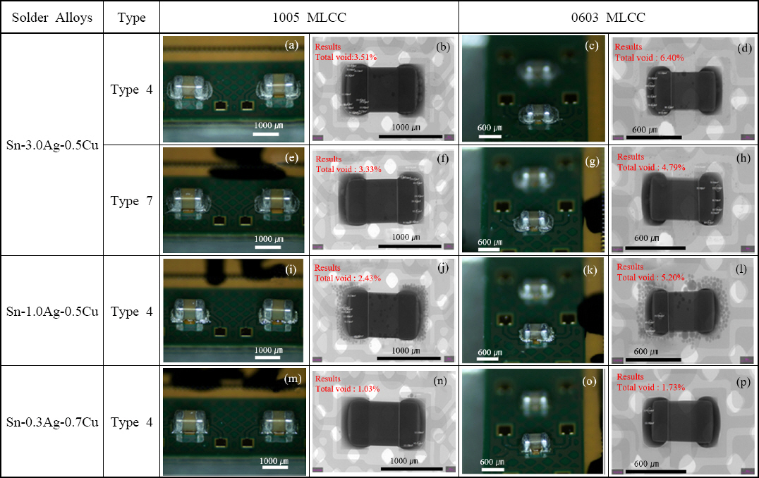
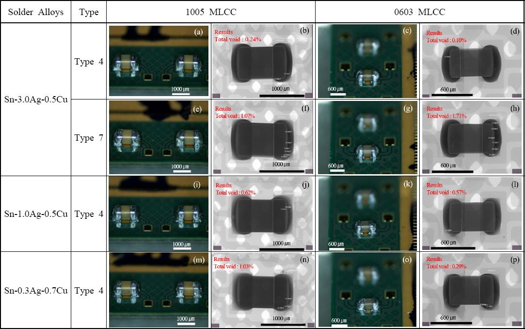
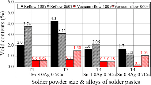
3.1 Void content of MLCC solder joints
Fig.┬Ā4
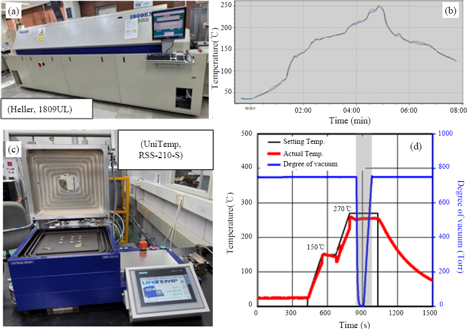
Fig.┬Ā5
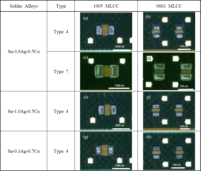
Fig.┬Ā6
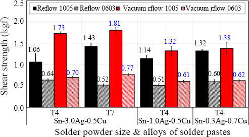
3.2 Bonding strength of MLCC solder joints
Fig.┬Ā9
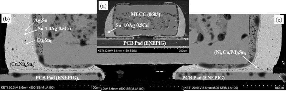
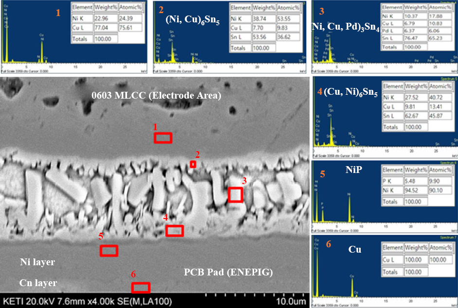
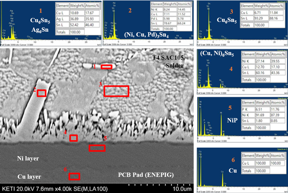
3.3 Analysis of solder joint interface
Fig.┬Ā10
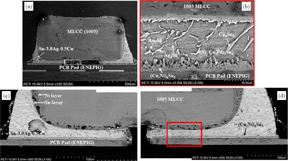
Fig.┬Ā11
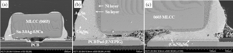
Fig.┬Ā12
4. Conclusion
1) Although the hot air reflow soldering process showed a stable void content in the joint at less than 5%, the application of the vacuum soldering process markedly reduced the void content of the solder joint. However, there was no significant difference in void content with respect to the powder particle size of the solder in the same bonding process. However, it is expected that if temperature profile suitable for the finer powder can be applied, superior bonding properties can be achieved.
2) In terms of the bonding strength of the SAC305 solder joint under the same powder size condition, the result from the use of hot air reflow soldering showed greater bonding strength than that from the use of vacuum soldering. This indicates that the vacuum soldering process is effective in removing voids during the void joining process, and the reduction in the void content contributed to the enhancement of the bonding strength of the solder joint.
3) With the application of the hot air reflow soldering and vacuum soldering process, the bonding strength of the T4 SAC305 solder joint was slightly higher than that of the SAC105 and SAC0307 solder, but the overall initial bonding strength was similar between the result values. Therefore, within the Ag content of 0.3-3.0 wt%, the effect on the initial bonding strength of SnAg-Cu solder is considered to be at the same level.
4) Various types of IMCs including Cu6Sn5, Ag3Sn, (Ni,Cu,Pd)3Sn4 (Cu,Ni)6Sn5, NiP, and Ni3P were formed on the interface between the ENEPIG finish substrate and SAC solder joint, and these IMCs are considered to contribute to the increase in the initial solder joint strength.
 PDF Links
 PubReader
 ePub Link
 Full text via DOI
 Download Citation
 Print
Print