1. Introduction
Wide-bandgap (WBG) semiconductors based on the compounds silicon carbide (SiC) and gallium nitride (GaN) are recently being commercialized. As with the full-scale development of highly efficient, high-frequency, highly reliable, and high power density power conversion systems (power modules such as inverters and converters) employing these compound semiconductors, the demand for WBG-based power modules is growing. Environmentally-friendly electric vehicles consume higher electric energy in comparison to previous internal combustion engines, for which an increase in the efficiency of power conversion is crucial. Therefore, a power conversion system such as an inverter or a converter, which converts the direct current (DC) and alternative current (AC) power conversion to the desired phase and frequency by using the properties of the power semiconductor, has become highly critical. Power modules for vehicle parts use high-power Si or SiC power semiconductors, for which demands are recently rapidly increasing. Therefore, the development of probe cards for power semiconductors, used in producing high-voltage and high-current power semiconductor elements, is simultaneously proceeded.
A probe card is utilized as a medium for signal transmission during the semiconductor manufactruring process, in the inspection for testing the electrical operation of the individual chips inside completed wafers. The probe card is a customized product, which is individually designed and fabricated to satisfy the specifications of the semiconductor for testing. It is classified as a high value-added product because a new probe card needs to be fabricated for each variation in the semiconductor specification. Additionally, the probe card is one of the core components for testing when the entire fabrication process, among the semiconductor production processes, is complete
1,2). Regarding the type of probe card for inspecting the state of the electrical operation of the chip inside the wafer, in which a precise line-shaped contact pin (or probe) adheres to the printed circuit board (PCB) of a certain standard. The probe contacts the wafer to serve as a medium between the measurement device and the wafer top surface and determine the fair to bad qualities of all the semiconductor chips. The cantilever wire probe card has long probes, for which evenly fitting the entire length of the probes is difficult. While it may limit high-speed signal transmissions, it is suitable for inspecting high-power and high voltage semiconductor elements such as the power semiconductor element. However, a probe card is repetitively used for wafer inspections, up to tens of thousands of times and with the potential tap (In/Out, I/O) on the surface of the power semiconductor wafer in contact with the wire, so the issue of sustained repetitive fatigue load delivered on the probe card wire arises. Accordingly, a fatigue fracture is generated due to the fatigue load on the bending part of the probe card wire, for which the development of wire materials improved for fatigue characteristics is being demanded. Additionally, the probe card wire during the measurement of the I/O on the wafer surface contacts with the touch-down (T/D) test method, which generates scrubs on the surface of the chip in the upper part of the wafer. Thus, the probe card wire must have outstanding bending strength and fatigue strength. Concurrently, the development of materials that do not cause scrub marks is in demand.
This study used four types of materials, tungsten (W), rhenium-tungsten (ReW), beryllium-copper (BeCu), and palladium-silver-copper alloy (P7, Pd-Ag-Cu) to measure the tensile strength of the probe card cantilever wire for power semiconductor wafer measurement and to comparatively analyze the fatigue properties of the wire according to the T/D fatigue test and the microstructural variations through the scanning electron microscopy (SEM) and electron back-scattered diffraction (EBSD).
2. Experimental methods
2.1 Cantilever probe wire material
The material properties and alloy type of the original material for the four types of cantilever wire probes are summarized in
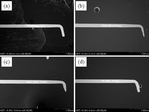
Table 1. W and ReW with high melting points and tensile strengths, and BeCu and Pd-Ag-Cu alloys with relatively low tensile strengths were used. The SEM images of the wire probes are shown in
Fig. 1. The tip diameter of the four wire probes W, ReW, BeCu, and P7 were 118, 43, 69, and 118 ŃÄø, respectively.
Table┬Ā1
Chemical composition and materials properties of cantilever wire probes
|
Cantilever wires |
Alloy composition |
Melting temperature (Ōäā) |
Density (g/cm3) |
Electrical resistivity (╬╝╬®┬Ęcm, 20Ōäā) |
|
W |
100% Tungsten |
3,410 |
19.24 |
5.59-5.86 |
|
ReW |
Rhenium-tungsten |
3,410 |
19.29 |
9.15-9.65 |
|
BeCu |
Beryllium copper |
925 |
8.4 |
7.0 |
|
P7 |
Palladium-silver-coper |
1,066 |
11.8 |
31.6 |
Fig.┬Ā1
SEM micrographs of cantilever wire probes, (a) W, (b) ReW, (c) BeCu and (d) P7
2.2 Cantilever wire tensile strength measurement
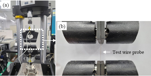
The tensile strengths of the four types of wire probes were measured using the Instron 8848 (Instron Co. Ltd., USA) equipment as shown in
Fig. 2. The grip with a serrated jaw face for testing the tensile strength was fixed to measure the tensile strength at 2 and 10 mm/min, and the degrees of influence to the testing velocity were compared.
Fig.┬Ā2
Photographs of (a) tensile test and (b) magnified images of wire probe
2.3 Scrub mark analysis and touch-down fatigue test
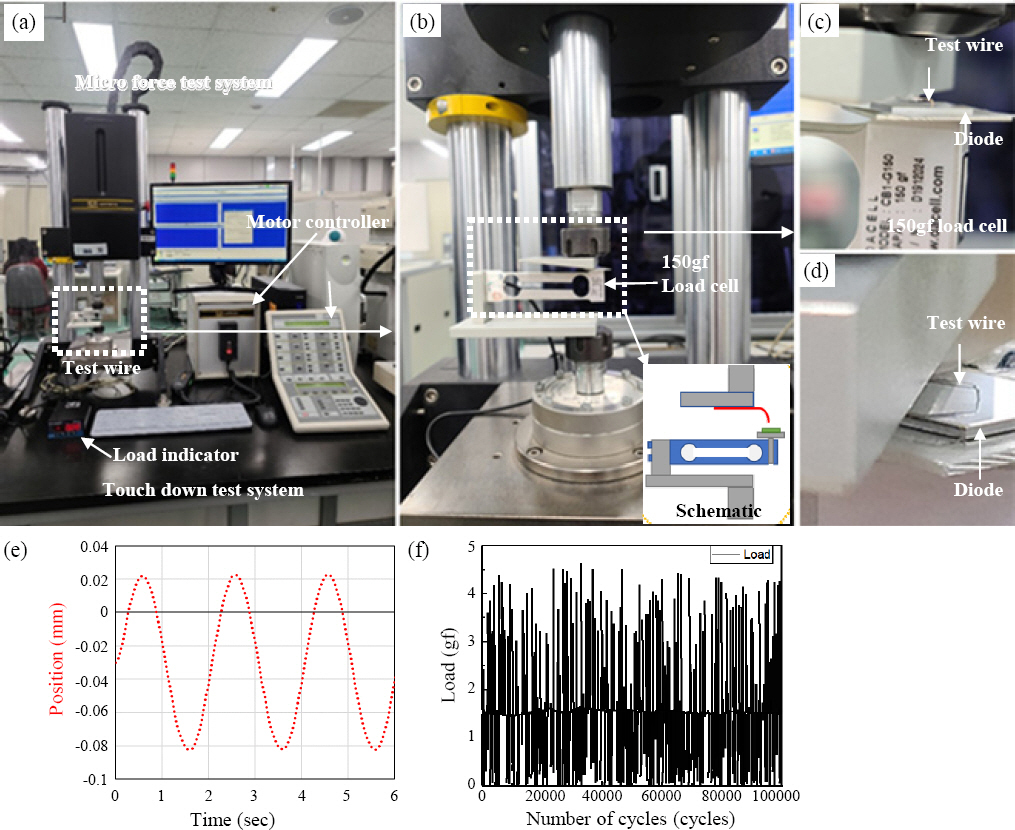
The size of the scrub marks generated on the chip surfaces were measured after one T/D to analyze the scrub marks generated during the power semiconductor element measurement with wire probes. The chip used in the experiment was a 9x9 mm diode (Trinno Technology Co. Ltd., South Korea) element used in power semiconductors, in which the chip surface was coated with a 4 ŃÄø aluminum (Al) thin-film. The scrub mark test proceeded with the application of a compressive load when the wire probe tip moved -80 ŃÄø from point of the contact on the chip surface, followed by the comparison of the sizes and lengths of the scrub marks generated on the diode surface.
Instron 8848 was used in the T/D fatigue test, similar to the scrub mark test, in which 100,000 test cycles proceeded as shown in
Fig. 3, with the conditions shown in
Table 2. During the T/D test, the test was set to be suspended at a 30% reduction in the fatigue load, considering the fracture generation in the wire probe. In addition, the wire was set to be 3.8 mm protruded from the wire fixing jig and fixed at a 7┬░ tilt, similar to the wire probe installed in an actual probe card, to proceed with 100,000 fatigue tests. The T/D fatigue test proceeded based on the displacement control. Here, loads of -10.5, 9.7, 5.35, and 7.4 gf were applied on W, ReW, BeCu, and P7 cantilever wire probes, respectively, with the -80 ŃÄø movement to the direction of compression. Since the range of compressive load is small, the load cell (CB1-G150, Dacell Co, Ltd., South Korea) with the maximum load range of 150 gf was used. The diode used in the T/D was fixed on the 150 gf load cell, and the fatigue test was set for the wire probe to repetitively touch down the diode surface. Here, the position of the repetitive motion of the device and the compressive load applied were monitored in real-time during the fatigue test. In the inspection with an actual probe card, the probe card movement inspects the power semiconductor wafer based on the -80 ŃÄø displacement rather than the load, so the fatigue test this experiment proceeded with a -80 ŃÄø displacement control as well. The -40 ŃÄø was set to the mean level to repetitively move the wire probe to its -80 ŃÄø objective, and the wire probe can repetitively move -80 ŃÄø when ┬▒40 ŃÄø is repetitively traveled back and forth. However, in this case, a non-contact condition between the wire probe and diode surface is not achieved, for which the test conditions were set to enable ┬▒50 ŃÄø movement based on -30 ŃÄø, as shown in
Fig. 3(e). The repetitive T/D frequency of the probe was set to 5 Hz.
Fig.┬Ā3
Photographs of T/D test set-up using by micro fatigue test system, (a) test system, (b) magnified view of fixed wire and load cell and (c,d) enlarged images of cantilever wire
Table┬Ā2
Fatigue test condition for T/D test of cantilever wire probe
|
Amplitude (ŃÄø) |
Mean level (ŃÄø) |
Frequency (Hz) |
Wave form |
Test cycles (cycles) |
|
50 |
-30 |
5 |
Sine Wave |
100,000 |
2.4 SEM and EBSD analysis
Before and after the T/D fatigue test, a cross-section of the wire probe and the angle of the bending part of the tip were measured. During the 100,000 cycles of fatigue tests, the SEM and EBSD analyses were performed to observe the bending part angle and the microstructural variations for each wire probe material. In particular, to observe the strain generated from the bending part microstructure and the grain orientation variations, the inverse pole figure (IPF), grain reference orientation deviation (GROD) maps, and the strain contouring maps were measured for comparative analysis.
3. Experimental results
3.1 Cantilever wire probe tensile strength measure- ment results
The tensile strength measurement results for the four types of wire probes are shown in
Fig. 4. They were 2.2-2.3, 1.9-2.3, 0.67-0.96, and 1.2-1.3 GPa for W, ReW, BeCu, and P7, respectively. The tensile strengths of W and ReW wires were measured to be higher than the wires containing Cu or Ag, while the toughness and elongation rate were measured to be higher in the BeCu and P7 wires. As shown in
Fig. 5, it can be seen that W and ReW showed brittle fractures and a mixture of ductile and brittle fracture modes, BeCu formed a ductile fracture plane, and brittle fractures were generated more in the P7. Thus, for the probe card, it is considered critical to select a wire probe material that has suitable fatigue strength and fatigue cycles from the repetitive T/D assessment.
Fig.┬Ā4
Tensile strength of 4 kinds of cantilever wire probes with test speed
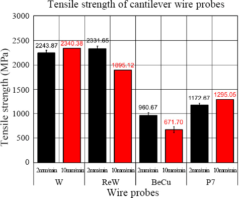
Fig.┬Ā5
Fracture surface SEM images of cantilever wire probes after tensile test, (a) W, (b) ReW, (c) BeCu and (d) P7
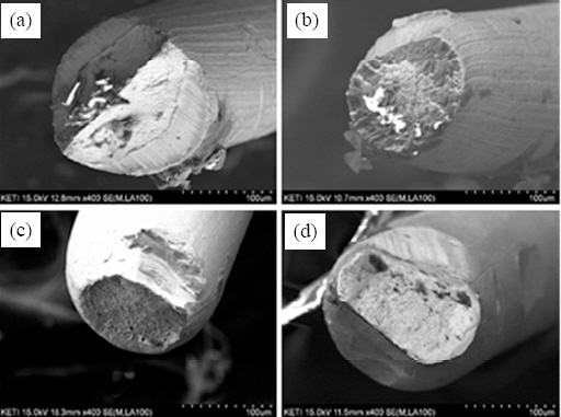
3.2 Scrub mark analysis results
The scrub mark sizes according to the wire probes were measured as 12.5, 25.6, 32.3, and 61.7 ŃÄø in W, ReW, BeCu, and P7, respectively. The W or ReW, which had high tensile strength measurements and aspects of brittle fractures from above, caused minimum scrub marks on the diode surface. In contrast, wire materials containing Cu had longer scrub marks and more contamination at the diode surface. Thus, W or ReW materials were considered to be beneficial for repressing the generation of scrub marks.
3.3 Cantilever wire microstructures after touch-down fatigue test
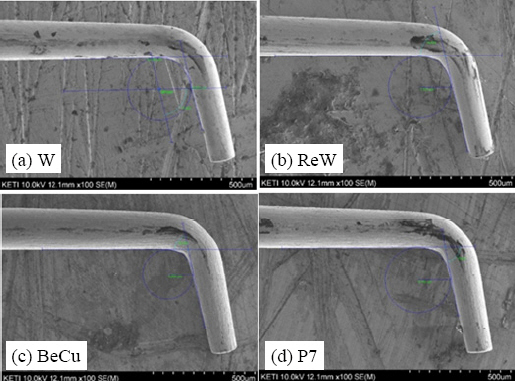
The measurement results of the bending angle of the wire bending part after the 100,000 T/D test that implements -80 ŃÄø displacement of the cantilever wire are shown in
Fig. 7. The measurements were 102┬░, 103- 104┬░, 102┬░, and 100-102┬░ in the W, ReW, BeCu, and P7 wires, respectively. Thereby, the P7 material showed the most wire deformation after the T/D fatigue test, followed by the BeCu wire. In comparison to the tensile strength assessment results, BeCu and P7 wires that have high elongation rates and tensile strengths showed larger deformations at the wire bending parts.
Fig.┬Ā6
SEM micrographs of scrub mark generated on the diode surface after 1 cycle T/D test, (a) W, (b) ReW, (c) BeCu and (d) P7
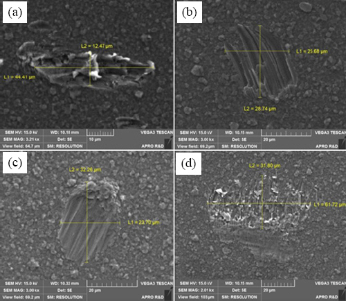
Fig.┬Ā7
SME images of cantilever wire probes after 100,000 cycles T/D fatigue test, (a) W, (b) ReW, (c) BeCu and (d) P7
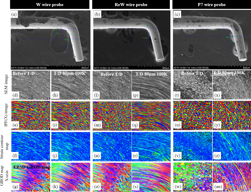
The SEM image and EBSD analyses results of the wire probe bending parts after the 100,000 T/D fatigue tests are shown in
Fig. 9. The variations of the deformed microstructures due to the repetitive tensile stress on the wire bending parts were comparatively analyzed using IPF images, GROD maps, and Strain contouring maps. Through IPF scanning images, the misorientation areas can be observed for the grain orientation, and the grain refinement or deformed areas can be distinguished. In the EBSD strain contouring map, plastic deformation can be located based on the localized misorientation areas, and the generation of the largest local plastic deformation can be located. In addition, through the EBSD GROD scanning, the residual stress area can be distinguished, and the relationship between the grain misorientation angle and the average grain orientation axis for all grains can be identified. The deformed microstructures in the wire probe bending parts were qualitatively compared through EBSD scanning analysis, which is shown in
Fig. 9.
Fig. 9(a) and (d-k) are the SEM and EBSD analyses results before and after the 100,000 T/D tests on the W wire probe,
Fig. 9(b) and (i-s) on the ReW wire probe, and
Fig. 9 (c) and (t-a╬▒) on the P7 wire probe. From the results of each specimen, it was identified that the grain at the bending part was elongated after the tests. This was identified to stem from the stress applied to the bending part during the repetitive T/D tests and to have elongated the bending part in the x-axis length di- rection. Additionally, the strain contouring map analysis results showed that there were more misorientation grains at the bending part. In the case of the W wire, the grain was longer than other wire microstructures before the tests but expanded even longer after the T/D tests. The fatigue resistance to such grain elongations or the resistance to fatigue stress is manifested as higher in materials with greater fracture toughness than tensile strength. Therefore, W and ReW with fundamentally high yield strengths are considered to have small deformations due to misorientations and strain generations from grain elongations, while materials with low yield strengths exhibit greater strain generations due to grain orientation deformations
3-8). Consequently, rather than those with high initial yield strengths, those with small deformations of the wire probe after long hours of use, namely ReW, W, and BeCu materials were considered to have superior touch-down fatigue characteristics to the P7 material.
Fig.┬Ā8
Bending angle comparison of cantilever wire probes before and after 100,000 cycles T/D fatigue test
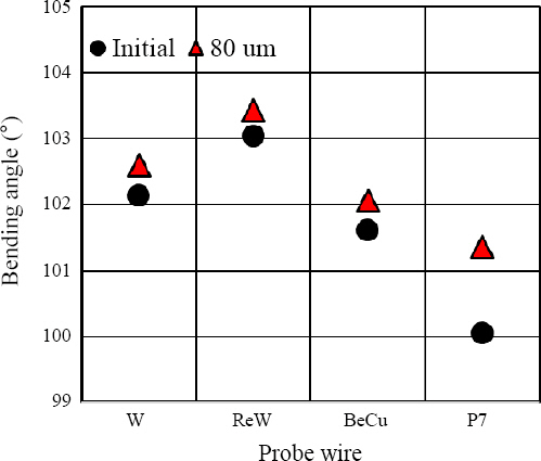
Fig.┬Ā9
SEM images and EBSD analysis results of bending area of cantilever wire probes after 100,000 cycles T/D fatigue test, (a) and (d-k) W, (b) and (i-s) ReW, and (c) and (t-a╬▒) P7
4. Conclusions
This study measured the tensile strengths and the scrub mark properties of the four types of cantilever wire probes that either used W, ReW, BeCu, or P7 alloys. Additionally, the fatigue characteristics of the wire and the variations in the microstructures according to the T/D fatigue tests were qualitatively and comparatively analyzed through SEM and EBSD scanning, which resulted as follows.
1) The wire probe tensile strength measurement results showed that they were high in W and ReW materials, and while the tensile strengths decreased in wires containing Cu or Ag, the toughness and elongation rates had increased. In W and ReW materials, brittle fractures and a mixture of ductile and brittle fracture modes were shown, BeCu formed a plane of ductile fracture, and more brittle fractures were generated in P7.
2) The results of measuring the bending angle of the cantilever wire bending parts after 100,000 T/D tests showed that the greatest deformation was in P7, followed by BeCu. In comparison to the yield strength results, bending part deformations were greater in BeCu and P7 materials that had high elongation rates and low tensile strengths.
3) In the W and ReW wire probes that had high initial yield strengths, the misorientation angle deformations due to the grain elongation were smaller than that in the P7 wire probe. Thereby, their grain deformations due to the generation of strains were lower, while materials with low initial yield strengths had larger strain generations due to the deformation of grain orientation. Therefore, long-term conditions of T/D use were considered to be superior in ReW, W, and BeCu than in P7, because deformations were small after a long period of use rather than having high initial tensile strengths.
Acknowledgements
This research was conducted with the funding from the Material and Components Technology Development Project (Project number: 20009828) supported by the Ministry of Trade, Industry and Energy.
References
1. Korea Institute of Science and Technology Information (KISTI).
Technical Tren of Semi-conductor Measurement and Inspection Equipment, The Ministry of Trade, Industry and Energy (MOTIE) and Materials &Component Technology Network (MCT-Net). Accessed on
https://www.mctnet.org(2020)
3. A. Palaniappan, L. Li, and T.-K. Lee, Impact of Press- fit Connector Pin Microstructure Elastic Response to PCB Through-hole Cu Wall Interface Long-term Contact Reliability,
Proc. 2018 IEEE 20th Electron. Packag. Techol. Conf. EPTC 2018. 890 (2018)
https://doi.org/10.1109/EPTC.2018.ŌćÄ324
[CROSSREF] 4. Y. J. Baek, A. Palaniappan, G. Baty, L. Li, S. K. Hyun, and T. K. Lee, Impact of Thermal Cycling on Cu Press- Fit Connector Pin Interconnect Mechanical Stability,
J. Electron. Mater. 50(11) (2021) 4991ŌĆō4998.
[CROSSREF] 5. L.N. Brewer, D.P. Field, and C.C. Merriman. Mapping and Assessing Plastic Deformation Using EBSD, Electron Backscatter Diffraction in Materials Science. In : Schwartz A.J, Kumar M, Adams B.L, Field D.P, editors. US, Boston, MA: Springer; (2009), p. 251ŌĆō262
https://doi.org/10.1007/s11664-021-09045-w
[CROSSREF] 7. W. S. Hong and C. Oh, PoF Based Accelerated Life Prediction with 3 Dimensional Packaging Technology Development,
J. Korean Weld. Join. Soc. 27(3) (2009) 10ŌĆō16.
[CROSSREF] 8. W. S. Hong and C. M. Oh, Thermal Shock Reliability of Low Ag Composition Sn-0.3Ag-0.7Cu and Near Eutectic Sn-3.0Ag-0.5Cu Pb-free Solder Joints, J. Korean Inst. Met. Mater. 47(12) (2009) 842ŌĆō851.


 PDF Links
 PubReader
 ePub Link
 Full text via DOI
 Download Citation
 Print
Print