Flip Chip - Chip Scale Package Bonding Technology with Type 7 Solder Paste Printing
Type 7 솔더 페이스트 프린팅 공정을 적용한 플립칩 - 칩 스케일 패키지 접합기술
Article information

Abstract
In this study, thermo-compression(TC) and vacuum reflow(VR) bonding processes of fine pitch interconnection were optimized using Type 7 Sn-3.0Ag-0.5Cu solder paste. A chip with Cu pillar Sn-2.5Ag bumps and BT substrate with ENEPIG surface finish were used, and the thickness and the aperture ratio of the metal mask were 30 ㎛/50 ㎛ and 70%/100%, respectively. As a result of optimizing the printing process, a metal mask with a thickness of 30 ㎛ and an aperture ratio of 100% was selected. As a result of the TC and VR bonding processes optimization, Cu₆Sn₅ and (Cu,Ni)₆Sn₅ IMC layers were formed on the top and bottom of the solder joint, respectively. In the conventional TC process sample, the thickness of the solder was measured to be 4.1 ㎛, and the IMC thickness ratio was calculated to be 40%. Also, in the TC and VR process samples with solder paste, the thickness of the solder was measured to be 6.5 ㎛ and 10.3 ㎛, respectively, and the ratio of the IMC thickness was calculated to be about 32% and 43%. It was expected that it would be beneficial to reliability by reducing the occurrence and propagation of cracks in the solder joint due to the effect of lowering the IMC thickness ratio as the volume of the solder becomes larger than that of the conventional TC process.
1. Introduction
The inputs and outputs (I/Os) of semiconductor packages are increasing and a high density of interconnections is being demanded as electronic products are becoming more functional and smaller. The semiconductor package interconnection technologies include wire bonding technology and flip chip bonding technology as shown in Fig. 1, which interconnects the electrodes of substrates by solder joint. The flip chip bonding technology can connect more I/Os than the wire bonding technology because it can use the front surface of the chip, and has the advantage of fast signal processing because the chip is approximately 10 times shorter than the wire length. Therefore, it is being applied in various ways for interconnection of high-density packages or digital packages that require fast signal processing1-5).

Schematic structural diagram of (a) wire bonding package, (b) flip chip-chip scale package (FCCSP) and (c) fine pitch FCCSP
For high-density I/O packages, it is necessary to research on the reduction of the pitch of joint bump. For bump sizes of 150 ㎛ or more, the printing process of solder paste, or solder balls are applied. If the pitch of the bump decreases to 150 ㎛ or less, electrical short circuit may occur due to solder bridge; hence, solder deposition or plating method is used as shown in Fig. 1 (c). Since the height of the joint decreases as the bump becomes smaller, it becomes difficult to achieve reliability and perform underfill at pitches of 140 ㎛ or less. Therefore, the Cu pillar bump technology that forms a Sn-based solder cap on a Cu pillar is applied at bump pitches of 140 ㎛ or less1-5).
Cu electrode pad and Cu pillar bump are joined, Cu- Sn-based intermetallic compounds (IMC) are formed. The smaller the bump size, the higher the percentage of IMC in the joint and the lower its reliability becomes. To improve this problem, the Ni-layer, which plays the role of preventing diffusion on a Cu electrode pad with a fine pitch, is formed by plating, or a Cu pillar bump plated with a highly reliable ternary solder is formed. However, ternary plating has the disadvantage of low mass production capacity due to a difficulty in plating solution management. Therefore, surface treatment methods such as electroless-nickel immersion-gold (ENIG) and electroless-nickel electroless-palladium immersiongold (ENEPIG) are mainly applied to the Cu electrode pad. In particular, the ENEPIG technology has been reported to have excellent mechanical reliability by suppressing the formation of kirkendall voids at the ENIG joint5-9).
This study optimized the thermo-compression (TC) bonding process of the flip chip-chip scale package (FC-CSP) using a chip with a Cu pillar Sn-2.5Ag bump of a 150 ㎛ pitch and an ENEPIG-surface-treated bismaleimide triazine (BT) substrate. In addition, this study investigated optimization of the thermo-compression (TC) bonding process and vacuum reflow (VR) bonding process, which applied a ternary lead-free solder using a type 7 Sn-3.0Ag-0.5Cu solder paste.
2. Experiment Method
2.1 Analysis of raw and subsidiary materials
The substrate used in this experiment was an ENEPIG- surface-treated BT substrate with a size of 15 × 15 mm as shown in Fig. 2. The substrate thickness was 0.3 mm, and the surface treatment thickness was 3-8 ㎛ for Ni, 0.05-0.15 ㎛ for Pd, and 0.05-0.15 ㎛ for Au. Regarding the chip, a 10 × 15 mm chip with 1,744 Cu pillar/Sn-2.5Ag bumps with a diameter of 90 ㎛, a pitch of 150 ㎛, and a height of approximately 50 ㎛ was used as shown in Fig. 3. For the solder paste, the composition of Sn-3.0Ag-0.5Cu (MKE Co. Ltd., Korea) was used, and the printing processability was evaluated using type 5 and type 7. As shown in Fig. 4, the solder ball sizes of type 5 and type 7 were 15-25 ㎛ and 2-11 ㎛, respectively.

Optical and SEM micrographs of BT substrate for FC-CSP, (a) top side and (b) magnified ENEPIG pad

Optical and SEM micrographs of Si flip chip, (a) bump side and (b) magnified Cu pillar bump

SEM micrographs of solder pastes, (a,b) Type 5 and (c,d) Type 7
2.2 Jig design and fabrication
A printing jig that can be fine-tuned for fine pitch solder paste printing was fabricated as shown in Fig. 5. The metal mask thicknesses were 50 ㎛ and 30 ㎛, and the opening ratios were 70 % and 100 %. The reflow bonding of the fine pitch FC-CSP chip requires a jog for aligning the bumps, and the jig was fabricated as shown in Fig. 6, in such a way that the FC-CSP chip can be fixed after printing. A jig that can fix the substrate was fabricated to suppress the generation of warpage at high temperatures due to the nature of BT substrate.

Photograph of Photograph of printing jig with X/Y/ θ axis adjustment for solder paste printing on the FC-CSP substrate
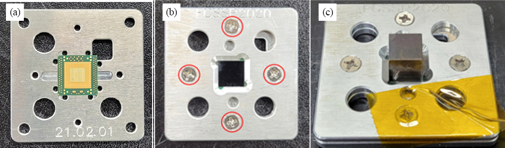
Photographs of vacuum reflow bonding jig, (a) Lower jig, (b) upper jig and (c) weight compression after the jig joining
2.3 Solder paste printing
The optimal solder paste and metal mask that do not cause defects such as bridge were selected by evaluating the printability of type 5 and type 7 solder pastes according to powder particle size, metal mask thickness, and opening ratio.
2.4 Thermo-compression bonding
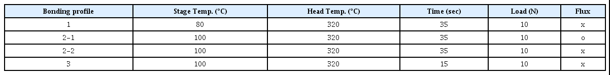
The thermo-compression (TC) bonding process used the flip chip bonder (NM-SB50A, Panasonic Co. Ltd., Japan). After bonding, the chip-substrate bonding condition was determined by measuring the electrical characteristics of all bumps connected to the daisy chain after bonding. The process conditions are listed in Table 1. As shown in Table 1, bonding profiles 2-1 and 2-2, void characteristics were evaluated by fabricating flux- applied sample and the un-applied sample. The TC bonding process of the chip with Cu pillar/Sn-2.5Ag bumps and the BT substrate were optimized. In addition, after the type 7 Sn-3.0Ag-0.5Cu solder paste and bonding were printed, the microstructures of the joints were compared.
The temperature and the pressure profile condition for thermo-compression bonding
2.5 Vacuum reflow bonding
The vacuum reflow (VR) bonding process used the RSS-210-S (UniTemp Co. Ltd., Germany) system with the process conditions in Fig. 7. As shown in Fig. 7 (e), the bonding profile was analyzed while changing the temperature rise rate, soak time, peak temperature and time. The temperatures on the jig surface were measured as shown in Fig. 7 (c). It started in nitrogen atmosphere and the vacuum atmosphere was formed in the peak temperature range, and cooling was performed by injecting nitrogen. During the bonding process, the bonding process was performed under a load of 0.18 N by pressurizing with an 18 g weight. Samples were fabricated for the case of pressurizing the top and bottom surfaces of the jig with screws and the case of no pressurizing, and the joints were compared.
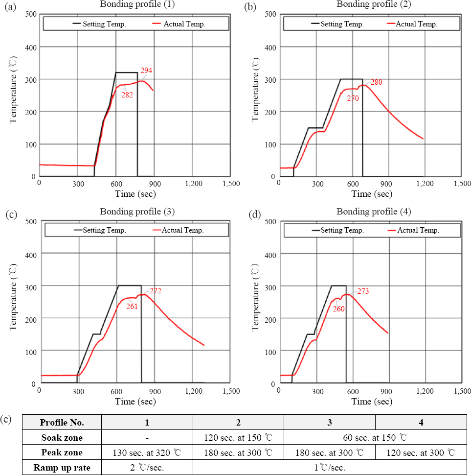
Bonding profiles of vacuum reflow bonding, (a-d) set and measured temperature and (e) profile condition
3. Experiment Results
3.1 Characteristics of printing process
The printing process results according to the solder paste type, metal mask thickness and opening ratio are shown in Fig. 8. When type 5 solder paste was printed, the solder ball did not fall out easily as shown in (a), and the printing was not done evenly when the 50 ㎛ metal mask was used. Finally, type 7 Sn-3.0Ag-0.5Cu solder paste and 30 ㎛ metal mask were selected, and they were printed with 70 % and 100 % opening ratios, respectively.
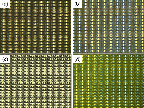
Optical micrographs after solder paste printing on the pad of BT substrate, (a) Type 5 solder paste, 30 ㎛ / 70% metal mask, (b) Type 7 solder paste, 30 ㎛ / 70% metal mask, (c) Type 7 solder paste, 50 ㎛ / 70% metal mask and (d) Type 7 solder paste, 30 ㎛ / 100% metal mask
3.2 Bonding characteristics of the thermo-compression bonding process
The bonding result of bonding profile 1 in Table 1 confirmed through the measurement of electric characteristics that no bonding was made. An observation of the fracture surface revealed that the bumps at the center of the chip were not melted. When the bonding was performed with bonding profiles 2 and 3 by increasing the stage temperature of the TC bonding system, the daisy chain resistance of bumps was measured at approximately 1 Ω or lower, thus we confirmed chip-substrate bonding, sucessfully. The result of X-ray analysis of samples fabricated under the conditions of bonding profiles 2-1 and 2-2 showed that there were less voids at the 2-2 joint without flux application as shown in Fig. 9. It was believed that more voids were formed by residues of flux due to the lack of flux reaction time. Furthermore, the fact that bonding profile 3 with a short bonding time showed the smallest number of voids suggest that more voids were formed inside as the solder spread more as the bonding time was longer. The bonding profile 3 was selected as the optimal condition, and the measured temperatures are shown in Fig. 10.
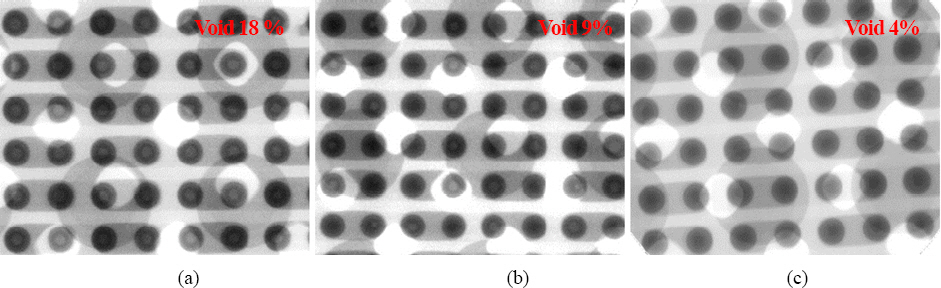
X-ray non-destructive analysis images after flip chip-BT substrate TC bonding using by (a) bonding profile 2-1, (b) bonding profile 2-2 and (c) bonding profile 3

The measured temperature of bonding profile 3
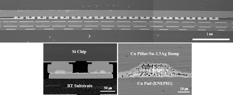
The cross-sectional analysis result of the bonding profile 3 sample showed that all bumps were bonded well at a constant thickness as shown in Fig. 11. However, when the cross-sections of the chip outline were observed, it was found that approximately a half of the Cu pillar joint was not filled due to insufficient solders as shown in Fig. 12 (a). In contrast, the cross-sectional analysis of the TC bonding to which solder paste printing was applied showed that the solder paste filled the entire area of the joint well and the bonding was performed well as shown in Fig. 12 (b). The EDS analysis result showed that a Cu₆Sn₅ IMC layer was formed on top of the joint and at the bottom, a (Cu,Ni,Au,Pd)₆Sn₅ IMC layer was sometimes observed, and it was mainly formed as a (Cu,Ni)₆Sn₅ IMC layer. The solder thickness was approximately 4.1 ㎛ at the joint of the chip outline, approximately 1.8 ㎛ at the top IMC, and approximately 0.9 ㎛ at the bottom IMC. After the solder paste printing process was applied, the solder thickness was approximately 6.5 ㎛ at the TC bonding, approximately 1.8 ㎛ at the top IMC, and approximately 1.2 ㎛ at the bottom IMC.
Cross-sectional SEM micrographs of FC-CSP bonded by profile 3
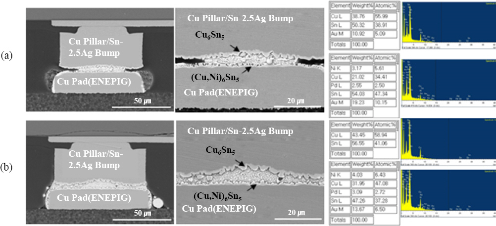
Cross-sectional SEM micrographs and EDS analysis results of thermal compression bonding profile 3 samples: (a) without solder paste and (b) with solder paste
3.3 Bonding characteristics of the vacuum reflow bonding process
Fig. 13 shows the cross-sectional analysis result of bonded samples (a) when the top and bottom surfaces were fixed with set screws and (b) when they were not fixed. For process condition, bonding profile 2 of Fig. 7 was applied. When the substrate was fixed with top and bottom jigs, the bump and pad aligned well. However, when a warpage of the BT substrate occur4red, it was found that the end of the substrat3e was not bonded as shown in Fig. 13 (a). In contrast, when the top and bottom jigs were fixed with screws, the joints were formed well at all bumps of the substrate as shown in Fig. 13 (b). This demonstrated that this jig fixing method is effective for suppressing the warpage of the BT substrate during the chip bonding process.

Cross-sectional SEM micrographs after the vacuum reflow bonding using by bonding
The X-ray analysis results of the joint according to the bonding profile in Fig. 7 are shown in Fig. 14. As a result of the X-ray analysis, fewer voids were observed at the joints of bonding profiles 3 and 4 with a shorter warm-up and peak temperature times.

X-ray non-destructive analysis images after the vacuum reflow soldered FC-CSP using by (a) bonding profile 1, (b) bonding profile 2, (c) bonding profile 3 and (d) bonding profile 4
Fig. 15 shows the cross-sectional analysis result of the joint by temperature profile. As a result of the EDS analysis, a Cu₆Sn₅ IMC layer was observed at the top, and a (Cu,Ni)₆Sn₅ IMC layer was observed at the bottom, the IMC grew rapidly according to the temperature and time of each bonding profile. Bonding profile 4 where micro-voids were not observed and the IMC thickness was the smallest was selected as the optimum condition. The solder thickness was approximately 10.3 ㎛ at the joint of the bonding profile 5 sample, approximately 6 ㎛ at the top IMC, and approximately 1.7 ㎛ at the bottom IMC.
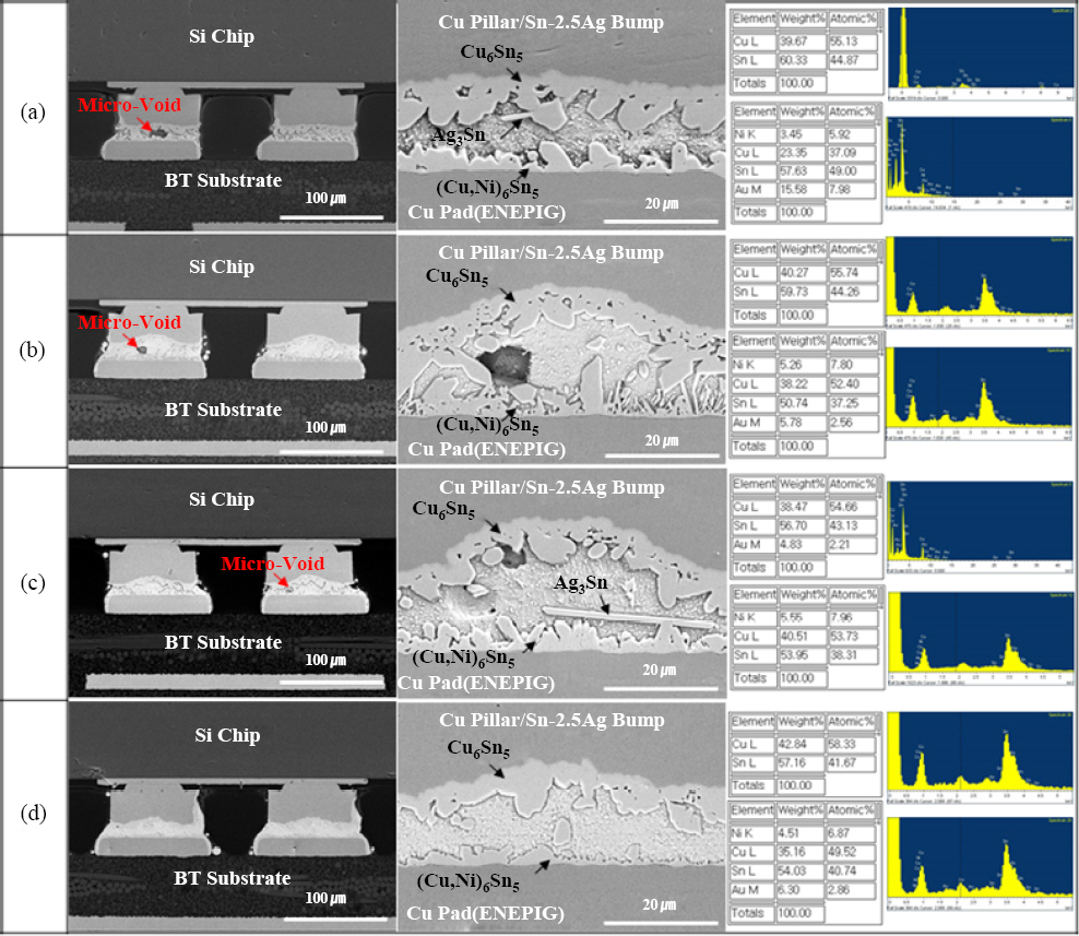
Cross-sectional SEM micrographs and EDS analysis results after the vacuum reflow soldered FC-CSP using by (a) bonding profile 1, (b) bonding profile 2, (c) bonding profile 3 and (d) bonding profile 4
By process, the solder thickness was 4.1 ㎛ at the TC bonded joint, 6.5 ㎛ at the TC bonded joint with solder paste printing applied, and 10.3 ㎛ at the VR joint. The IMC thickness ratio to the total joint was approximately 40% at the TC bonded joint, approximately 32% at the TC bonded joint with solder paste printing applied, and approximately 43% at the VR joint. According to previous studies, cracks at the TC bonding were caused by ductile failure due to fatigue and spread through micro-voids due to creep, and the cracks of IMC were mainly caused by brittle failure along the interface of Cu₆Sn₅ or Cu₃Sn10). Furthermore, it has been reported that the larger the solder volume at the joint, the lower the generation and spread of cracks at the joint, thus improving fatigue life11). Therefore, it was considered that the VR joint with the largest solder volume and the TC bonding with printing applied, which had the lowest ratio of the IMC thickness, would be more advantageous for reliability than the joint of the conventional TC process. Furthermore, it was also considered that if the VR process temperature was lowered further, the reliability could be improved more effectively.
4. Conclusions
This study optimized the thermo-compression bonding process of FC-CSP using a chip with Sn-2.5Ag capped Cu pillar bumps of 90 ㎛ diameter and an ENEPIG-surface-treated BT substrate. TC bonding and VR bonding were performed, and the TC and VR bonding processes of the ternary solder were optimized by applying the printing process of type 7 Sn-3.0Ag-0.5Cu solder paste.
1) The result of optimizing the printing process using type 5 and type 7 solder pastes, and metal masks of 30 ㎛ and 50 ㎛-thicknesses and the opening ratios of 70 % showed that type 7 solder paste and the metal mask with 30 ㎛ thickness and 100% opening ratio were most appropriate.
2) The bonding process was optimized by applying TC bonding with flip chip-BT substrate bonding process, TC bonding with solder paste printing process, and VR bonding process. A Cu₆Sn₅ IMC layer was formed at top of the joint, and a (Cu,Ni)₆Sn₅ IMC layer was formed at the bottom. The thicknesses of the solder joint were 4.1 ㎛, 6.5 ㎛, and 10.3 ㎛, respectively, and the IMC thickness ratios were approximately 40 %, 32 %, and 43 %, respectively.
3) The result of the TC and VR bonding processes with type 7 solder paste printing showed that the solder volume increased compared to the conventional TC process and this had an effect of decreasing the IMC thickness ratio. This was considered to be advantageous for reliability by decreasing the generation and spread of cracks due to the effect of lowering the IMC thickness ratio resulting from the increased solder volume compared to the conventional TC process.
Acknowledgments
This research was conducted with the funding from the Material and Components Technology Development Project (Project number: 20011427) supported by the Ministry of Trade, Industry and Energy.