


1. Introduction
2. Experimental Method
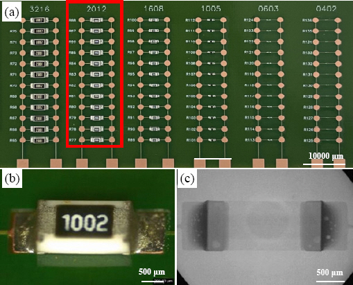
2.1 Creating samples to evaluate solder paste properties
Table┬Ā1
| Solder pastes | A | B | C |
|---|---|---|---|
| Flux chemical type | Rosin | Aqueous (Water soluble) | Rosin |
| Liquid flux content (wt%) | 12 | 12 | 13 |
| Solder powder content (wt%) | 88 | 88 | 87 |
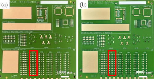
Fig.┬Ā2
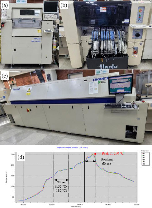

2.2 Thermal shock test (TST)
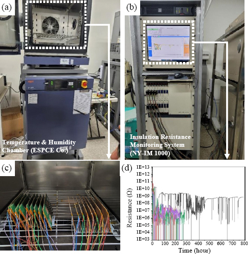
2.3 Electrochemical metallic ion migration (ECM) test
2.4 Measuring solder joint void content and bond strength
3. Experimental Results
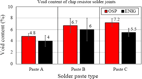
3.1 Measuring the solder joint void
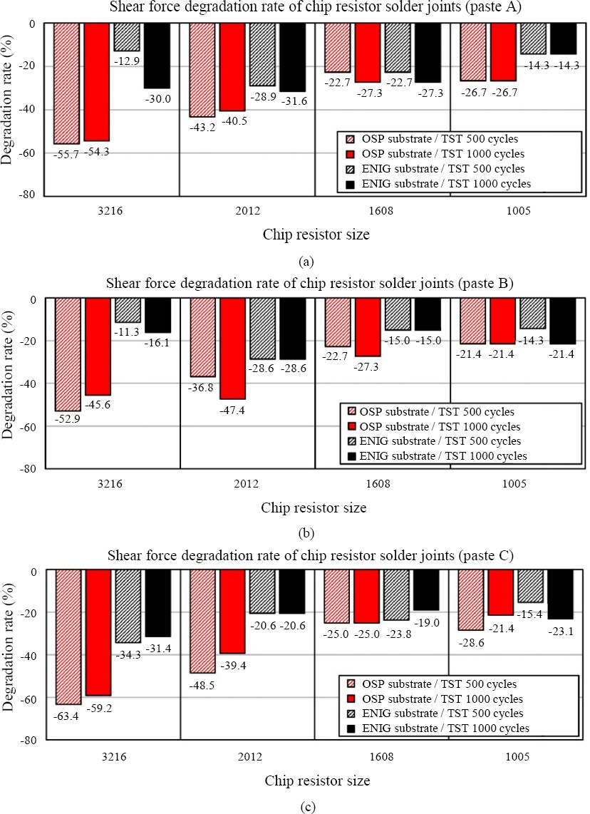
3.2 Solder joint shear test assessment

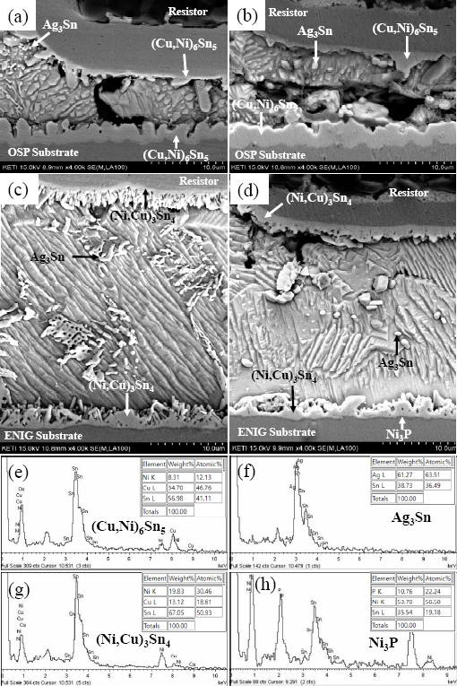
3.3 Analyzing the microstructure of solder joint
Fig.┬Ā9
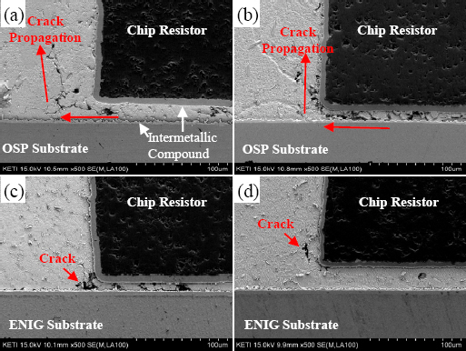
Fig.┬Ā10
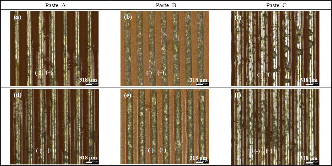
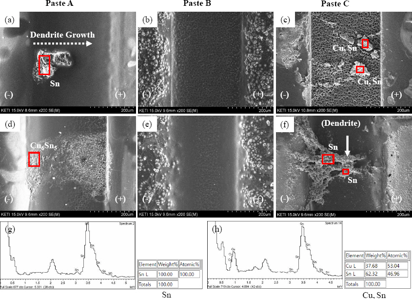
3.4 ECM test result
Fig.┬Ā11
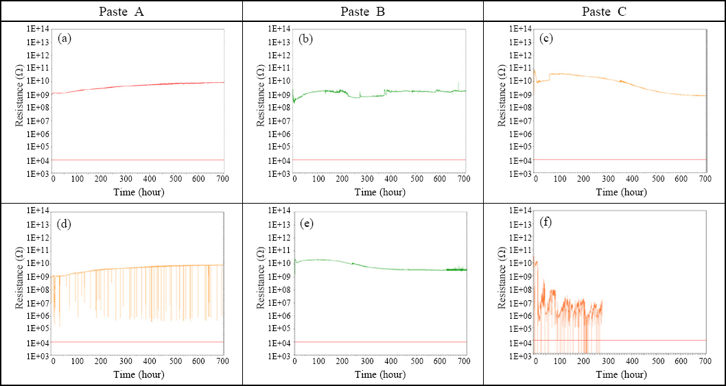
Fig.┬Ā12
4. Conclusions
1) The solder joint void content of the 2012 chip resistors showed a higher void content on the OSP than on the ENIG substrate. The OSP surface finish substrate showed a higher void content than the ENIG substrate because the organic film evaporated during reflow and formed voids inside the solder.
2) The bonding strength of chip resistors after nitrogen reflow was not significantly changed by surface finish, but the degradation rate was measured higher on the OSP than the ENIG substrate after TST. The cross-sectional analysis revealed that the OSP had more advanced crack morphology and thicker IMCs than the ENIG substrate, which explained the higher degradation rate measurement.
3) After ECM test, more dendrites developed on the substrate with PSR compared to the substrate without PSR. It was determined that the substrate with PSR was responsible for more dendrites due to the inhibition of the release of moisture absorbed into the substrate.
 PDF Links
 PubReader
 ePub Link
 Full text via DOI
 Download Citation
 Print
Print