


1. Introduction
With the rising functionality of electronic products, the number of I/Os in semiconductor packages is increasing, and this requires a high density of inter- connections. The upper package in Fig. 1 shows the interconnection technology that connects the chip and substrate with wires, which is referred to as wire bonding. In wire bonding, the chip and substrate are bonded in one dimension. However, flip-chip bonding, in which the chip is turned over and bonded to the substrate, as shown in the lower package in Fig. 1, is suitable for bonding chips with a large number of I/Os because metal pads are arranged on the entire area of the chip. Furthermore, the length of the junction of flip- chip bonding is tens of micrometers, which is about 10 times shorter than the wire length of wire bonding, resulting in fast signal processing of electronic products. Consequently, flip-chip bonding technology is widely applied in digital fields that require high-speed signal processing1-3).
Fig.┬Ā1
Schematic structural diagram of package-on-package with wire bonding package as an upper package and fine pitch flip-chip chip-scale package as a lower package

As the density of the I/O in the package increases, the pitch of the bump at the junction decreases. Various bump formation techniques are applied depending on the bump pitch. When the bump pitch is 150 ŃÄø or more, the process of applying solder balls or printing solder paste is applied. For packages with a bump pitch of 150 ŃÄø or less, there is difficulty in applying the printing process due to the uniformity of the bump resulting from the problem of the loosening of the solder paste. When the packageŌĆÖs pitch is 140 ŃÄø or less, it is better to use a bump with a copper pillar rather than a solder bump to ensure reliability and stable underfill. Flip-chip bonding is possible by forming a solder such as SnAg on the Cu pillar by electroplating process1-3).
Various bonding process technologies are applicable depending on the bump pitch of these semiconductor packages. Flip-chip bonding processes include reflow and thermal compression (TC). The reflow process is prone to device misalignment and shorting when the bump pitch is small. To address these issues, the TC process is used to bond the devices. However, the TC process has the disadvantage of poor mass production because the devices are individually joined by applying heat and pressure (Fig. 2)1-3).
Fig.┬Ā2
Thermal compression bonding process, (a) chip mounting on the substrate, (b) thermal compression bonding with pressing and heating

To overcome the limitations of bump pitch refinement in these packages, a highly integrated package-on- package (PoP) technology has been developed that forms interconnections between packages by stacking packages on top of each other as shown in Fig. 1,4,5). Each upper and lower package of a PoP package can selectively contain passive elements such as inductors, multi-layer ceramic capacitors (MLCCs), and other packages depending on the application to realize a high-performance package. Si chips and passive devices in a package generally use a TC bonding process for Si chips and a hot air reflow process for passive devices, so mounting both Si chips and passive devices in a package requires two separate processes. If chips and passive devices are simultaneously bonded using reflow, it can be shortened to a single process. Further- more, the vacuum reflow (VR) process is a reflow method that maintains a vacuum in the peak temperature region. This increases the fluidity of the voids in the peak temperature region and reduces the void content of the joint. Simultaneous joining using this VR process can improve the reliability of the joint compared to hot air reflow. Previous research has demonstrated the possibility of simultaneous VR bonding of chips and MLCCs using Sn-3.0Ag-0.5Cu solder paste6).
The VR process is a method of printing a paste on a substrate, mounting the chip, and then reflowing it (Fig. 3). If formic acid is added to remove the solderŌĆÖs native oxide film during the VR process for chips with SnAg- plated Cu fillers, the printing process can be omitted and the chips can be joined (Fig. 4). Studies on VR soldering using formic acid have been conducted before7-12).
Fig.┬Ā3
Vacuum reflow soldering process with additional solder paste, (a) BT substrate with copper post, (b) solder paste printing on the substrate, (c) chip mounting on the substrate and (d) vacuum reflow soldering
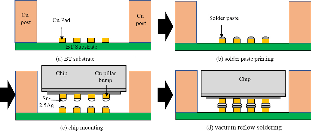
Fig.┬Ā4
Vacuum reflow soldering without paste, (a) BT substrate with copper post, (b) chip mounting on the substrate without solder paste printing and (c) vacuum reflow soldering with formic acid atmosphere

Therefore, the solder joint characteristics of chips bonded by TC bonding and the VR process under a formic acid atmosphere were compared in this study. Si chips with Sn2.5Ag solder cap plating on the Cu filler bumps and no solder paste on the Cu filler bumps for package bonding were placed on the substrate and then bonded by TC bonding and VR process in a formic acid atmosphere. Voids, bond strength measurements, and microstructure analysis were performed to compare the bonding characteristics of the solder joints of the chips after bonding. In addition, scanning electron microscopy (SEM) and energy dispersive spectroscopy (EDS) were performed to examine the intermetallic compound (IMC) formed at the solder joints.
2. Experiment Method
2.1 Used Materials
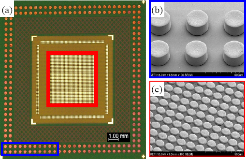
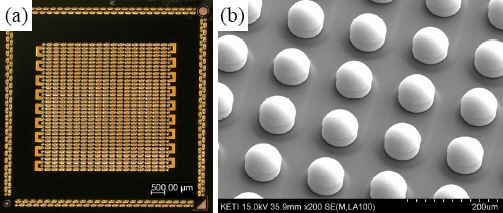
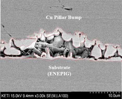
A bismaleimide triazine substrate (BT substrate) with an area of 15 ├Ś 15 mm and a thickness of 0.3 mm was used in this study, as shown in Fig. 5 (a). The surface treatment of electroless-nickel electroless-palladium immersion-gold (ENEPIG) was applied to this substrate. The surface treatment thickness was 3-8 ŃÄø, 0.05-0.15 ŃÄø, and 0.05-0.15 ŃÄø for Ni, Pd, and Au, respectively. As shown in Fig. 5 (b, c), a copper post with a diameter of 300 ŃÄø, a height of 150 ŃÄø, and a pitch of 500 ŃÄø formed at the corner of the substrate for the PoP junction with the upper package was analyzed by SEM and the substrate pad with ENEPIG surface treatment. As shown in Fig. 6 (a), a Si chip with an area of 0.8├Ś0.8 mm was used. The shape of the solder bump on the chip was confirmed by scanning electron microscopy and the result is shown in Fig. 6 (b). The diameter, pitch, and height of the solder bump were 75 ŃÄø, 130 ŃÄø, and 60 ŃÄø, respectively. The Cu pillar bump was plated with a Sn-2.5Ag solder capping with a thickness of 30 ŃÄø over a 30 ŃÄø Cu filler.
2.2 Thermal compression bonding (TC bonding)
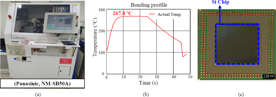
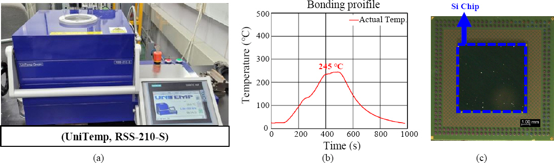
The Si chip was mounted on the BT substrate and bonding was performed using the TC bonding equipment (Panasonic, NM-SB50A) shown in Fig. 7 (a). For the bonding process, a pressure of 1 kgf (10 N) was applied for 20 s at a peak temperature of 267.8 ┬░C. Fig. 7 (b) shows the temperature profile conditions applied to the TC bonding process. After the bonding process, the samples were analyzed for appearance as shown in Fig. 7(c). The daisy chain resistance of the flip-chip chip- scale package (FC-CSP) sample bonded by TC bonding showed a stable value.at approximately 1 ╬®.
2.3 Vacuum reflow soldering (VR soldering)
After the Si chip was mounted on the BT substrate, the process was performed using the VR process equipment (RSS-210-S, Unitemp Co., Germany) illustrated in Fig. 8 (a). A bonding jig was used to align the bumps and pads of the chip, and the process was carried out in a vacuum atmosphere with a peak temperature of 245 ┬░C for 900 seconds. Fig. 8 (b) shows the temperature profile conditions used in the VR bonding process, and a photomicrograph of the sample after bonding is shown in Fig. 8 (c). The resistance of the daisy chain of the FC-CSP sample without formic acid could not be measured, confirming that it was not bonded. This is considered to be due to Cu oxidation on the CuAg plating. To address this issue, formic acid was added to the preheating section from 150 ┬░C to 180 ┬░C. The resistance of the daisy chain of the sample with formic acid was measured and found to be less than 1╬®, which confirmed the stable bonding of the chips.
2.4 Measurement of solder joint void content and cross-sectional analysis
The solder joint void content of the samples with TC bonding and VR soldering without solder paste application was measured using an X-ray non-destructive analysis equipment (Xslicer SMX-6000, Shimadzu Co., Japan). Furthermore, the junction interfaces of TC- bonded and VR-bonded samples were analyzed by SEM and EDS.
2.5 Measurement of solder joint IMC thickness and area fraction
The thickness of the IMC of the solder joints joined by TC and VR processes and the area fraction of the IMC relative to the joint area were calculated and compared. As shown in Fig. 9, the area of the IMC surrounded by the red lines on the top and bottom of the joint was set as the measurement area. The thickness and area fraction of the IMC were calculated according to the following Equations 1 and 2.
(1)
3. Experimental Results and Discussion
3.1 Analysis of solder joint void
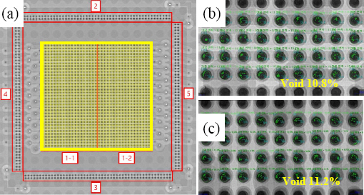
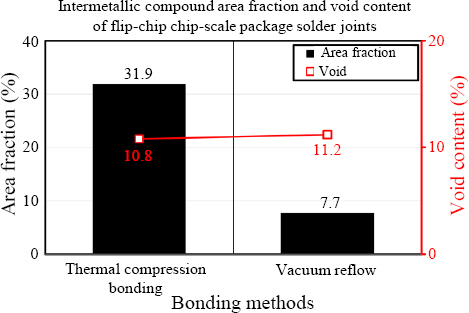
The void content of the solder joints corresponding to the yellow area in Fig. 10 (a) was measured and the results are shown in Fig. 10 (b). The void contents of the TC bonding and VR soldering joints were 10.8% and 11.2%, respectively, indicating that the VR soldering process can realize joint properties similar to those of TC bonding without additional solder paste application. The low void content of each sample is attributed to the increased void fluidity in the package bump solder joints due to the pressurization during the TC bonding process and the vacuum atmosphere in the VR process.
3.2 Cross-sectional microstructural analysis of solder joints
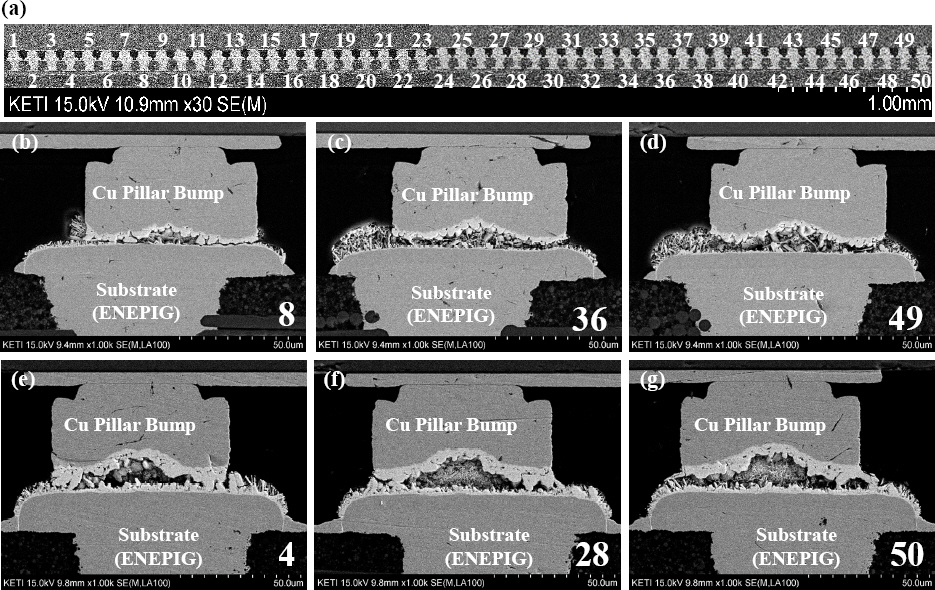
Cross-sectional microstructure analysis was conducted to verify the thickness and IMC of the solder joints. The cross-sectional analysis of the solder joints of the samples bonded by TC bonding and VR process with formic acid is shown in Fig. 11 and Fig. 12 with SEM photographs. In addition, the solder joints of the package bumps were numbered 1-50 sequentially from the left side of the solder joints in Fig. 12 (a). It was confirmed that compared to the samples bonded by TC bonding in Fig. 12 (b-d), the samples bonded by the VR process with formic acid in Fig. 12 (e-g) had thicker joints. It was determined that the thickness of the joint was thinner than that of the VR process because the TC bonding process uses high pressure to stably bond the bumps on the chip.
Fig.┬Ā11
SEM cross-sectional micrographs of FC-CSP solder joints with (a) thermal compression bonding and (b) vacuum reflow soldering
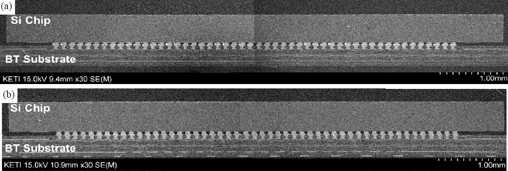
Fig.┬Ā12
(a) FC-CSP solder bump numbering image from left side and SEM cross-sectional micrographs of (b) 8th, (c) 36th, (d) 49th solder bumps with thermal compression bonding and of (e) 4th, (f) 28th, (g) 50th solder bumps with vacuum reflow soldering
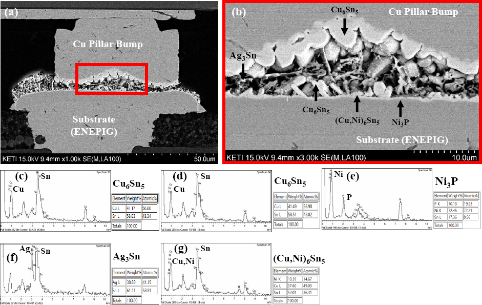
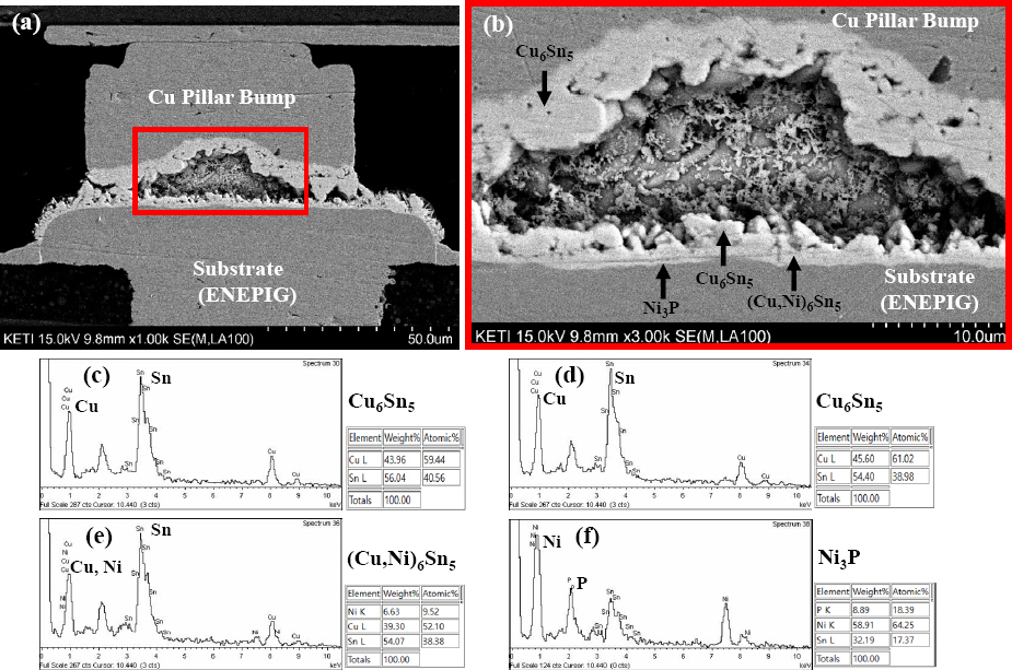
The IMCs formed at the solder joints of the samples subjected to TC bonding and VR processes were analyzed by EDS, and the results are shown in Fig. 13 and Fig. 14, respectively. It was found that Cu6Sn5 and (Cu, Ni)6Sn5 IMCs were formed in the upper and lower parts of the solder joints of the TC bonding samples, as shown in Fig. 13(c), (d), and (g). The formation of Ag3 Sn IMC in the parent material part of the solder joint was confirmed, as shown in Fig. 13 (f). This was determined to be formed by the Sn-2.5Ag solder cap-plated Ag elements in the solder bump13). Furthermore, Ni3P was observed at the interface of the lower IMC and the substrate pad, as shown in Fig. 13(e). It was concluded that the Ni in ENEPIG and the Phosphorous (P) in the electroless Ni plating on the substrate pad were used14). In the upper and lower parts of the joints of the VR soldered joint samples, Cu6Sn5 and (Cu, Ni)6Sn5 were found by the Sn-2.5Ag solder cap of the solder bump, as shown in Fig. 14 (c), (d), and (e). At the interface of the lower IMC substrate pad part, Ni3 P was formed by ENEPIG surface treatment, as shown in Fig. 14 (f).
3.3 Analysis of IMC thickness and area fraction of solder joints
The calculation results of IMC thickness and area fraction of solder joints are outlined in Tables 1 and 2. As shown in Table 1, the IMC thickness of the solder joints of the TC bonding sample was 8.0 ŃÄø, and the IMC thickness of the VR process with formic acid was 19.2 ŃÄø. It was found that the IMC thickness of the VR process sample was larger. However, as shown in Table 2, the area ratio of the IMC to the total solder joint was 31.9% for the TC bonding sample and 7.7% for the VR process sample, indicating that the IMC area ratio of the VR process sample was smaller. This is attributed to the larger area of the solder joints in the VR process sample, compared to the TC bonding sample. The graph comparing the void and IMC area fraction is shown in Fig. 15. According to previous research, the IMC thickness in the VR sample was greater than in the TC bonding sample. However, after 500 cycles of TC, the VR bonding process with a larger area of the solder joints was superior to the TC bonding sample in terms of reliability6). Despite the thicker formation of IMC in the VR bonding sample, it is considered that the bonding reliability is superior because the area of the IMC is smaller than the area of the solder joints.
Table┬Ā1
Intermetallic compound thickness of FC-CSP solder bumps with thermal compression bonding with vacuum reflow bonding
4. Conclusions
In this study, the bonding characteristics of flip-chip bumps using the VR process in a formic acid atmosphere and the TC process were compared, and the results are as follows.
1) The solder joint void content of the TC and VR process samples was 10.8% and 11.2%, respectively. It is thought that the voids in the TC process were caused by the pressurization during processing and the vacuum atmosphere in the VR process.
2) The joint area of the chip was thinner because the TC process pressurized the bumps on the chip at a high pressure to reliably bond them. Consequently, the IMC area fraction of the solder joint of the Cu pillar bump was smaller for the VR process sample than for the TC process sample.
3) The above results suggest that the VR process in a formic acid atmosphere can achieve simultaneous bonding of passive devices and Si chips with a 130 ŃÄø bump pitch.
 PDF Links
 PubReader
 ePub Link
 Full text via DOI
 Download Citation
 Print
Print