


Bonding Property of Middle Temperature Sn-Ag-Cu Solder Ball Joint of Ball Grid Array Package
-
Joo Young Bae*
 , Mi-Song Kim*, Hye Min Lee*, Seul Gi Lee**, Young-Woo Lee**, Jeong Tak Moon**, Won Sik Hong*,†
- Received August 4, 2023 Revised September 4, 2023 Accepted September 8, 2023
- ABSTRACT
-
Alloying effects of Nickel and Bismuth in SAC solder to achieve mechanical and microstructural evolution were investigated by comparing three different chemical composition of solders. Sn-3.0Ag-0.5Cu (SAC305) is the most commonly used for Pb-free solder and solder balls are based on Sn-Ag-Cu alloy composition. Compositions of solder balls were Sn-3.0Ag-0.5Cu (SAC305), Sn-1.2Ag-0.5Cu-0.05Ni (SAC1205N) and Sn-Ag-Cu-Ni-Bi based solder (SACNB). Organic solderability preservative (OSP) surface finished substrate, ball grid array (BGA) package arranged by 300 ㎛ diameter solder ball and Type 4 solder paste were used. Solder ball shear test of the BGA package was conducted before the reflow soldering. Board level package bonding process was carried out by hot air reflow soldering. Void content of the BGA solder joint was investigated after soldering. The microstructure evolution before and after thermal cycle test (TCT) was observed using scanning eletron microscopy (SEM) and energy dispersive spectroscopy (EDS). After TCT, intermetallic compound (IMC) refinement and solid solution strengthening effects of Bi element addition were observed in the solder matrix, and also any segregation of Bi element was not founded. Based on these result, it was found that the solder joint reliability of the middle and low temperature solder joints was improved.
- 1. Introduction
- 1. Introduction
In recent years, the semiconductor packaging field has been demanding advanced Pb-free solder alloys with improved impact resistance and thermal cycling reliability compared to conventional Sn-Ag-Cu (SAC) alloys. In response to this demand, there has been active research on the development of Pb-free solder alloy compositions and bonding reliability based on trace element additions in SAC alloy formulations1,2). According to previous research, the reflow peak temperature for typical Sn-Ag-Cu solder is in the range of 245-260 °C, but it can be lowered to below 200°C by using Bismuth (Bi)-based solder paste. Therefore, the addition of Bi serves as the foundation for the development of low-melting-temperature solder (LTS)3). With the decrease in process temperature, it becomes possible to reduce warpage caused by the coefficient of thermal expansion (CTE) mismatch between materials, thereby mitigating thermal deformation of electronic components and soldering defects. This reduction in process temperature also holds the promise of improving manufacturing yields in surface mounting technology (SMT) and achieving energy and cost savings4,5). Furthermore, when Bi is added in trace amounts rather than exceeding the 2 wt% threshold that can induce precipitation, it is expected that Bi is incorporated into the Sn-rich matrix, resulting in solid solution strengthening effects.In this study, we conducted a comparative analysis of solder joint characteristics by incorporating small quantities of alloying elements, including Ni and Bi, into the widely used Pb-free solder, Sn-Ag-Cu. Specifically, we introduced 1 wt% Bi to lower the melting point and prevent Bi precipitation. The solder balls used were of three compositions: Sn-3.0Ag-0.5Cu (SAC305), Sn- 1.2Ag-0.5Cu-0.05Ni (SAC1205N), and Sn-2.5Ag-0.8Cu- 0.05Ni-1.0Bi (SACNB). Ball grid array (BGA) package components with these three compositions were assembled using organic solderability preservative (OSP)- finished substrates and Type 4 SAC305 solder paste through a hot air reflow soldering process. We then conducted solder ball shear tests to compare bonding strength for each composition and measured void fractions following the board-level soldering process. Subsequently, we conducted a thermal cycling test (TCT) comprising 1,000 cycles to verify bonding reliability and performed microstructure analysis before and after the TCT. The procedure described above is visually represented in Fig. 1.

- 2. Experimental Methods
- 2. Experimental Methods
- 2.1 Materials and Sample Preparation
- 2.1 Materials and Sample Preparation
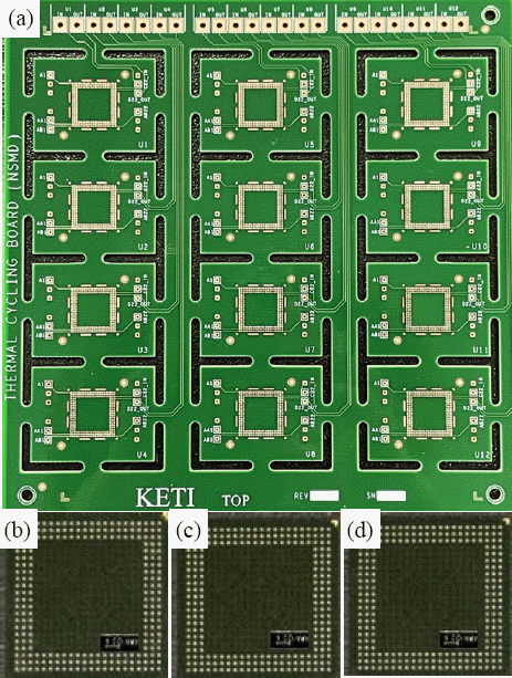
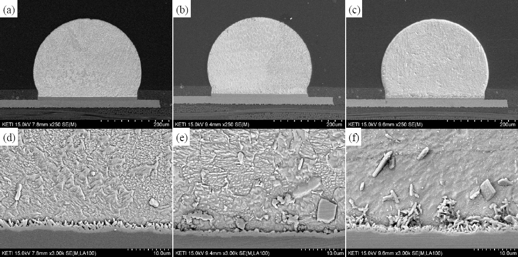
For the experiments, we prepared experimental board- level package bonding coupons using printed circuit boards (PCBs) treated with OSP, which had a thickness of 0.25-0.45 ㎛ and dimensions of 127×125 mm (Fig. 2(a)), along with Type 4 SAC305 solder paste and BGA packages (Fig. 2 (b-d)). To investigate variations in bonding characteristics resulting from the addition of trace alloying elements in SAC solder balls, we utilized SAC305, SAC1205N, and SACNB alloy compositions to fabricate board-level coupons (Fig. 3 (a-c)). According to the analysis of the cross-sections of the BGA packages depicted in Fig. 3 (d-f), it is evident that SAC305 and SACNB formed faceted-type intermetallic compounds (IMCs), while SAC1205N exhibited a flat IMC structure. This observation suggests that SAC1205N, due to the presence of Ni within the base material, had limited diffusion from the Ni pad into the base material, resulting in the formation of a flat IMC.- 2.2 Hot Air Reflow Soldering Process
- 2.2 Hot Air Reflow Soldering Process
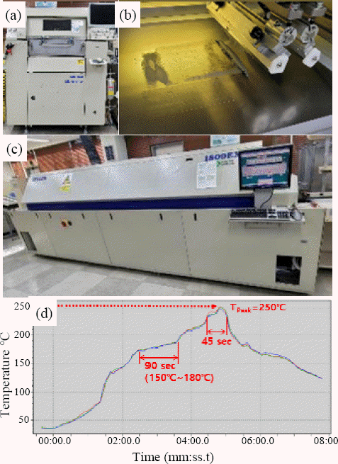
Using a screen printer (MK-878Mx, Minami Co. Ltd., Japan) as shown in Fig. 4(a), we conducted the SAC305 solder paste printing process, as depicted in Fig. 4(b), followed by mounting the BGA and carrying out the reflow process. The soldering process was carried out using a hot air reflow soldering machine (1809UL, HELLER Co., USA) as illustrated in Fig. 4(c). The temperature profile, as shown in Fig. 4(d), included preheating at 150-180°C for 90 seconds, followed by maintaining the maximum temperature at 250 °C for 45 seconds during the soldering process. The fabricated samples resulting from the process are presented in Fig. 5.- 2.3 Ball Shear Strength Testing of BGA Package Solder Joints
- 2.3 Ball Shear Strength Testing of BGA Package Solder Joints
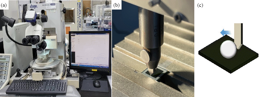
Ball shear strength tests were carried out on the solder ball joints of BGA package components for each composition prior to the reflow soldering process. The tests were performed using the bonding test equipment (Dage 4000, Nordson Co. Ltd., UK) at a test speed of 500 ㎛/s and a shear test jig height of 20 ㎛, as shown in Fig. 6(a)-(c).- 2.4 Void Fraction Analysis of Solder Joints After Reflow Soldering
- 2.4 Void Fraction Analysis of Solder Joints After Reflow Soldering
Void content in the solder joints was measured after the reflow soldering process. Non-destructive X-ray analysis (X-slicer, SMX-6000, Shimadzu Co., Japan) was employed to inspect the alignment and bonding state of solder ball joints, and the void fraction relative to the solder joint area was determined.- 2.5 Thermal Cycling Test
- 2.5 Thermal Cycling Test
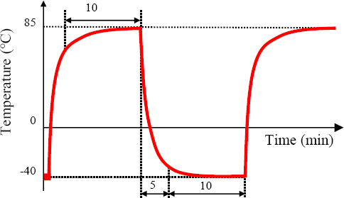
To assess the reliability of the BGA package joints, a TCT was conducted under the test conditions, which included 1,000 cycles with a temperature range of -40 to 85°C and a 10-minute dwell time, as shown in Fig. 7. The microstructural changes in the cross-sections before and after the TCT were observed using scanning electron microscopy (SEM) and energy dispersive spectroscopy (EDS). We further assessed the thickness and distribution of the IMC and measured crack length after the TCT.

- 3. Results and Discussion
- 3. Results and Discussion
- 3.1 Shear Strength of Solder Balls in Ball Grid Array Packages
- 3.1 Shear Strength of Solder Balls in Ball Grid Array Packages
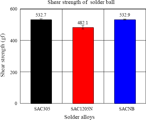
The results of the shear strength tests on solder ball joints in BGA packages in Fig. 8 revealed that SAC305 and SACNB exhibited similar strengths, with values of 532.7 gf and 532.9 gf, respectively, while SAC1205N displayed the lowest shear strength at 482.1 gf. According to previous research, the addition of trace amounts of Bi, around 1 wt%, does not significantly affect shear strength compared to cases where higher Bi content of 2-3 wt% is present. Hence, it was observed that the shear strength values of SAC305 and SACNB were similar with the addition of Bi in the range of 1 wt%6).- 3.2 Void Fraction in Solder Ball Joints
- 3.2 Void Fraction in Solder Ball Joints
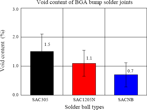
The results of the void fraction measurements at the joints between the package and PCB after BGA package assembly (Fig. 9) showed that SACNB exhibited the lowest void fraction at 0.7%, while SAC1205N and SAC305 had increased void content at 1.1% and 1.5%, respectively. In the case of SACNB, due to the lower melting point resulting from the addition of Bi compared to SAC305, solder melting and bonding take precedence under the same reflow soldering process conditions. Consequently, it is presumed that voids were effectively eliminated after the solder balls and paste reached a molten state and achieved sufficient wetting, resulting in a low void fraction.- 3.3 Microstructure of Solder Joints After TCT
- 3.3 Microstructure of Solder Joints After TCT
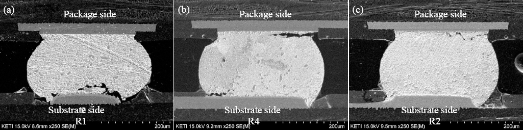
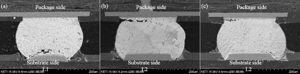
Fig. 10 and 11 depict the SEM cross-sectional analysis results of the solder joints on the right and left sides of the chips in the BGA package after 1,000 cycles of TCT. The formation of cracks and their propagation behavior in solder joints are influenced by various factors such as solder ball composition, warpage, surface treatment, and board design. In terms of the initiation points of cracks in the solder ball joints, it was observed that cracks started at the PCB solder joint and propagated into the base material along the IMC interface in the case of SAC305. In contrast, for SAC1205N and SACNB, cracks predominantly initiated at the ends of the package joints and progressed toward the center of the base material.- 3.4 IMC Thickness and Crack Length
- 3.4 IMC Thickness and Crack Length
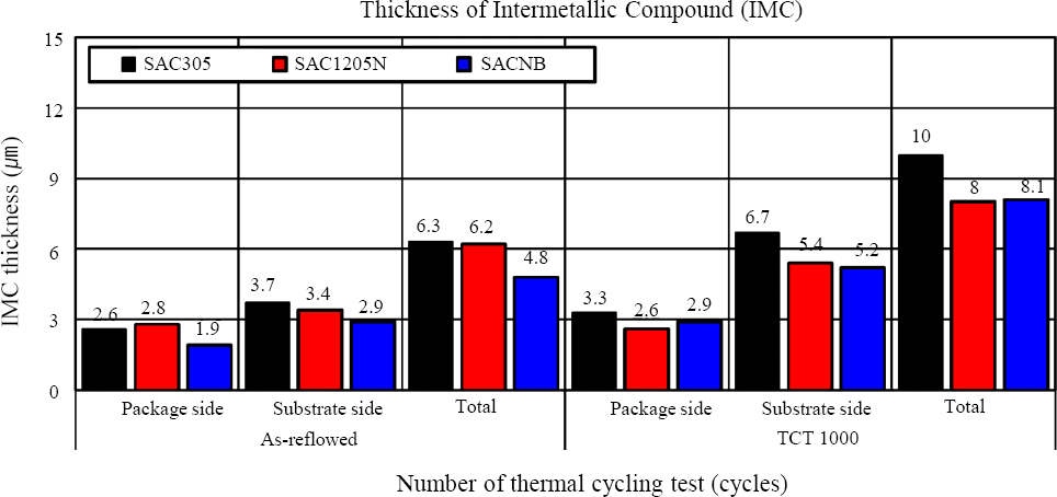
Fig. 12 presents the analysis results of IMCs formed in the joints. After the reflow process, (Cu,Ni)6Sn5 was predominantly formed at the BGA package side joints due to the Ni plating on the bumps (Figs. 12 (a-c)). In contrast, the PCB side joints exhibited Cu6Sn5 formation due to OSP surface treatment (Figs. 12 (d-f))7). The formation of IMCs in solder joints is a significant factor that compromises joint reliability due to their brittleness. (Cu,Ni)6Sn5 is more stable and relatively easier to form compared to Cu6Sn5 due to its lower free energy8), and the Ni and Cu elements are redistributed during the formation of (Cu,Ni)6Sn59). Ni and Cu elements in the vicinity of the interface are consumed during TCT cycles, resulting in the formation of depletion zones that tend to facilitate crack initiation. Therefore, it is determined that cracks in the solder ball joints at both ends of the BGA package bumps occurred in areas close to the joint interface, as shown in Figs. 10 (b,c) and Figs. 11 (b,c)10).Fig. 12
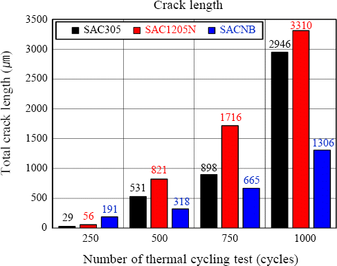
SEM micrographs of solder joints : (a-c) as-reflowed package side SAC305, SAC1205N and SACNB, (d-e) as reflowed substrate side SAC305, SAC1205N and SACNB, (g-i) after TCT 1000 cycles package side SAC305, SAC1205N and SACNB, (j-l) after TCT 1000 cycles substrate side SAC305, SAC1205N and SACNB Regarding the PCB-side solder joints, cracks were observed to initiate at the end of the PCB pads. The pad design on the PCB side is based on the solder mask defined (SMD) approach, and SMD design is presumed to exhibit crack behavior similar to the results of our experiments, as cracks tend to initiate and propagate from the solder mask location during creep deformation11).Fig. 13 presents the results of IMC thickness measurements after the bonding process and following 1000 cycles of TCT. IMC thickness was calculated by dividing the total IMC area shown in Fig. 12 by the width at which IMC was formed12). For Cu6Sn5 IMC formed on the PCB-side joints with SACNB, the thickness was the lowest at 5.2 ㎛, while those with SAC1205N and SAC305 had thicker layers at 5.4 ㎛ and 6.7 ㎛, respectively. With the advancement of the TCT cycle, the increase in IMC thickness led to a reduction in joint strength due to decreased fatigue life, resulting in crack initiation13). The addition of Ni elements to low-Ag SAC alloys is known to suppress the formation of Cu3Sn IMC that occurs between Cu and Cu6Sn5, leading to thinner IMC layers14). Therefore, SAC1205N and SACNB, both of which incorporate Ni as an additive, demonstrate increased brittleness, reducing the probability of fracture as the formation of cracks along the IMC is inhibited14). Bi has also been reported in previous studies to inhibit Cu3Sn growth15). For these reasons, it is speculated that the addition of trace elements inhibited the formation and propagation of cracks along the IMC layers within the solder joint interface.The results of solder ball joint crack length measurements in Fig. 14 showed that SACNB exhibited the shortest crack length. Although SACNB initially had a relatively long crack length of 191 ㎛ after 250 TCT cycles, the increase in crack length with TCT cycles was not significantly pronounced. After 1000 cycles, SACNB had a crack length of 1,306 ㎛, which was significantly better in thermal cycle reliability compared to SAC305 and SAC1205N, which had crack lengths of 2,946 ㎛ and 3,310 ㎛, respectively. This improved thermal reliability is attributed to the effective suppression of crack propagation in solder joints due to the solid solution strengthening effect resulting from the addition of trace amounts of Ni and Bi in SAC-based solder alloys16). Bi solute atoms, which are larger than Sn atoms (RBi=156 pm, RSn=140 pm), form compressive strain fields within the Sn matrix, inhibiting plastic deformation17).
- 4. Conclusion
- 4. Conclusion
In this study, we compared the reliability of joints with the addition of trace alloying elements using three different solder compositions. The comparison of crack propagation patterns revealed that SACNB exhibited the shortest crack length, whereas SAC1205N had the longest measured crack length. When comparing crack length, void fraction, and shear strength, it was determined that SACNB, with trace additions of Ni and Bi at < 2 wt%, demonstrated the most stable solder joint reliability. This improvement in solder joint reliability is attributed to the solid solution strengthening effect of SAC-based alloy compositions due to the addition of Ni and Bi.
- Acknowledgments
- Acknowledgments
This research was conducted with the support of the Ministry of Trade, Industry, and Energy’s Global Key Technology Development Program for Root Technology Development (Project No. 20018332).
- REFERENCES
- REFERENCES
References
1. Md. Mahmudur, R. Chowdhury, M. A. Hoque, A. Fahim, C. S. Jeffrey, . Sa'd Hamasha, and P. Lall, Microstructural evolution in SAC305 and SAC-Bi solders subjected to mechanical cycling. International Electronic Packaging Technical Conference and Exhibition, American Society of Mechanical Engineers. 51920 (2018) https://doi.org/10.1115/IPACK2018-8414
[Article]2. J. Pan, J. Wang, and D. M. Shaddock, Lead-free solder joint reliability-State of the art and perspectives, J. Microelectron. 2(1) (2005) 72–83. https://doi.org/10.4071/1551-4897-2.1.72
[Article]3. Y. W. Lee, T. K. Lee, and J. P. Jung, Intermediate Low- elting-Temperature Solder Thermal Cycling Enhancement Using Bismuth and Indium Microalloying, J. Electron. Mater. 52 (2023) 810–818. https://doi.org/10.1007/s11664-022-10121-y
[Article]4. S. Mokler, R. Aspandiar, K. Byrd, O. H. Chen, S. Walwadkar, . Kok, and et al, The application of Bi-based solders for low temperature reflow to reduce cost while improving SMT yields in client computing systems, Proceedings of SMTA International. (2016)5. H. Kang, B. Baek, and J. P. Jung, Recent Low Temperature Solder of SnBi and Its Bonding Characteristics, J. Weld. Join. 38(6) (2020) 576–583. https://doi.org/10.5781/JWJ.2020.38.6.8
[Article]6. Y. Chen, Z. C. Meng, L. Y. Gao, and Z. Q. Liu, Effect of Bi addition on the shear strength and failure mechanism of low-Ag lead-free solder joints, J. Mater. Sci:Mater Electron. 32 (2021) 2172–2186. https://doi.org/10.1007/s10854-020-04982-4
[Article]7. S. Kim, W. Hong, H. Nam, and N. Kang, Growth Behavior of Intermetallic Compounds in Various Solder Joints Induced by Electromigration, J. Weld. Join. 39(1) (2021) 89–102. https://doi.org/10.5781/JWJ.2021.39.1.11
[Article]8. T. K. Lee, H. Ma, K. C. Liu, and J. Xue, Impact of Isothermal Aging on Long-Term Reliability of Fine- Pitch Ball Grid Array Packages with Sn-Ag-Cu Solder Interconnects:Surface Finish Effects, J. Electron. Mater. 39 (2010) 2564–2573. https://doi.org/10.1007/s11664-010-1352-8
[Article]9. S. W. Fu, C. Y. Yu, T. K. Lee, K. C. Liu, and J. G. Duh, Impact crack propagation through the dual-phased (Cu,Ni)6Sn5 layer in Sn-Ag-Cu/Ni solder joints, Materials Letters. 80 (2012) 103–105. ISSN 0167-577Xhttps://doi.org/10.1016/j.matlet.2012.04.099
[Article]10. T. K. Lee, B. Zhou, T. Bieler, and K. C. Liu, Impact of Microstructure Evolution and Isothermal Aging on Sn-Ag-Cu Solder Interconnect Board-Level High-G Mechanical Shock Performance and Crack Propagation, J. Electron. Mater. 41 (2012) 273–282. https://doi.org/10.1007/s11664-011-1775-x
[Article]11. H. Ma and T. K. Lee, Effects of Board Design Variations on the Reliability of Lead-Free Solder Joints, in IEEE Transactions on Components, Pack. Manufac. Technol. 3(1) (2013) 71–78. https://doi.org/10.1109/TCPMT.2012.2223214
[Article]12. J. Yoo, S. Kim, W. S. Hong, and N. Kang, Intermetallic Compound Growth Induced by Electromigration in Sn-2.5Ag Solder Joints with ENEPIG Surface Finish, J. Weld. Join. 40(3) (2022) 225–232. https://doi.org/10.5781/JWJ.2022.40.3.3
[Article]13. J, Y. Park, M. S. Kim, C. Oh, S. H. Do, J. D. Seo, D. K. Kim, and W. S. Hong, Solder Joint Fatigue Life of Flexible Impact Sensor Module for Automotive Electronics, Korean J. Met. Mater. 55(4) (2017) 232–239. https://doi.org/10.3365/KJMM.2017.55.4.232
[Article]14. A. Syed, T. S. Kim, Y. M. Cho, C. W. Kim, and M. Yoo, Alloying effect of Ni, Co, and Sb in SAC solder for improved drop performance of chip scale packages with Cu OSP pad finish, 2006 8th Electronics Packaging Technology Conference, Singapore. (2006) 404–411. https://doi.org/10.1109/EPTC.2006.342750
[Article]15. E. Hodúlová, M. Palcut, E. Lechovič, B. Šimeková, and K. Ulrich, Kinetics of intermetallic phase formation at the interface of Sn-Ag-Cu-X (X=Bi In) solders with Cu substrate, J. Alloy. Compd. 509(25) (2011) 7052–7059. ISSN 0925-8388https://doi.org/10.1016/j.jallcom.2011.03.164
[Article]16. J. Zhao, L. Qi, X. Wang, and Wang. Lai, Influence of Bi on microstructures evolution and mechanical properties in Sn-Ag-Cu lead-free solder, J. Alloy. Compd. 375(1-2) (2004) 196–201. https://doi.org/10.1016/j.jallcom.2003.12.005
[Article]17. S. H. Hu, T. C. Lin, C. L. Kao, F. Y. Huang, Y. Y. Tsai, S. C. Hsiao, and J. C. Kuo, Effects of bismuth additions on mechanical property and microstructure of SAC-Bi solder joint under current stressing, Micro- electron Reliab. 117 (2021) 114041https://doi.org/10.1016/j.microrel.2021.114041
[Article]